High-sensitivity in-cell touch display device

a touch display device, high-sensitivity technology, applied in the direction of instruments, computing, electric digital data processing, etc., can solve the problems of degrading display quality, degrading parasitic capacitance, and disadvantageous additional volume and weight of the touch panel, so as to improve the sensing distance, stable and consistent voltage, and reduce parasitic capacitance

Active Publication Date: 2016-09-15
SUPERC TOUCH CORP
View PDF2 Cites 14 Cited by
  • Summary
  • Abstract
  • Description
  • Claims
  • Application Information

AI Technical Summary

Benefits of technology

[0007]The object of the present invention is to provide a high-sensitivity in-cell touch display device, which can provide a touch circuit with a touch-dedicated independent power supply circuit and use a common voltage and sensing electrode as a common node of the touch circuit and a display circuit. Thus, there is no current loop between the touch circuit and the display circuit, so that the relative voltage level of the display circuit has no influence to the relative voltage level of the touch circuit. In addition, reflective deflection electrodes are provided to reduce parasitic capacitance between the common voltage and sensing electrodes and to improve the sensing distance, thereby providing relatively stable and consistent voltage for the common voltage and sensing electrode. As a result, the disturbance to the display quality caused by the touch operation can be minimized, and a display operation and a touch sensing operation can be performed on different areas in parallel so as to increase respective efficiencies of the display and touch sensing operations.

Problems solved by technology

A typical touch display device is provided by mounting a touch panel on a display panel with a complicated process and high material cost, which relatively reduces the light penetration rate and thus degrades the display quality.
In addition, the additional volume and weight of the touch panel are disadvantageous to the trend of compactness and energy conservation and emission reductions for electronic devices.
In the aforementioned typical in-cell touch display panels, when the resolution of the screen is increased, the display operation is difficult to have enough time for a touch sensing operation.
Likewise, when the size of the screen is enlarged, the number of touch points is relatively increased and thus more time is required to scan the touch sensing electrodes.
Accordingly, time division becomes difficult, resulting in that the resolution of the in-cell touch screen is limited and the size of the screen is restricted.

Method used


Image

  • High-sensitivity in-cell touch display device
  • High-sensitivity in-cell touch display device
  • High-sensitivity in-cell touch display device

Examples


Embodiment Construction

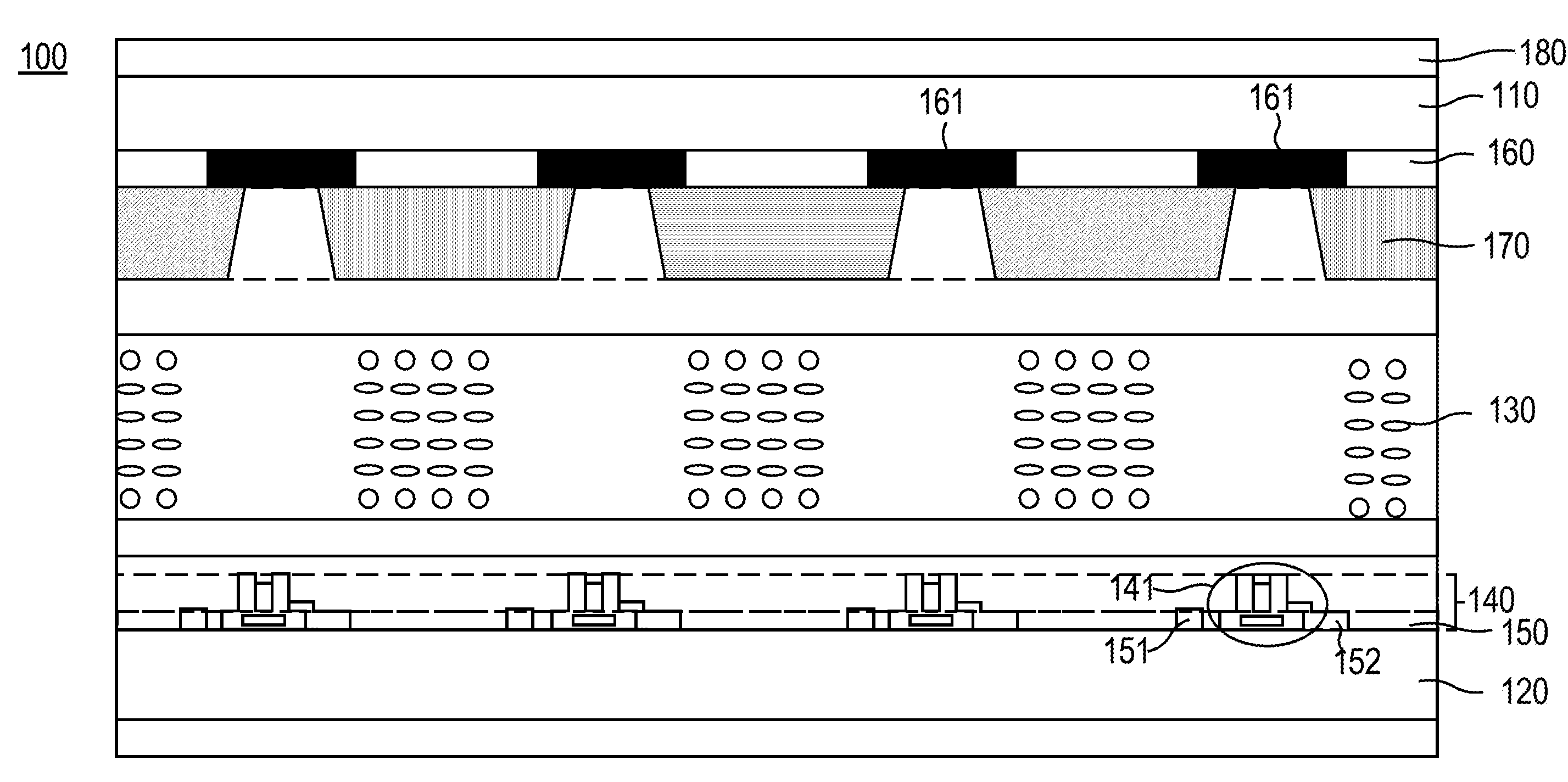
[0019]FIG. 1 schematically illustrates a stacked diagram of a high-sensitivity in-cell touch display device 100 according to the invention. The high-sensitivity in-cell touch display device 100 includes a first substrate 110, a second substrate 120, a display material layer 130, a thin film transistor (TFT) layer 140, a common voltage and sensing electrode layer 150, a black matrix layer 160, a color filter layer 170, and a polarization layer 180.

[0020]The first substrate 110 and the second substrate 120 are preferably glass or polymer thin film substrates. The first substrate 110 and the second substrate 120 are arranged in parallel and the display material layer 130 is disposed between the first and second substrates 110, 120. In this embodiment, the display material layer 130 is a liquid crystal layer.

[0021]The TFT layer 140 is arranged on one surface of the second substrate 120 facing the display material layer 130. The TFT layer 140 is provided with a plurality of thin film tra...


PUM


Abstract

A high-sensitivity in-cell touch display device has a common voltage and sensing electrode layer including a plurality of common voltage and sensing electrodes, each corresponding to at least one pixel electrode. A touch circuit is provided with a touch-dedicated power supply circuit, and a common voltage and sensing electrode is used as a common node of the touch circuit and a display circuit, so that there is no current loop between the touch circuit and the display circuit. Reflection electrodes are further provided to reduce parasitic capacitance between the common voltage and sensing electrodes and to improve the sensing distance. The display operation and the touch sensing operation can be performed on different areas in parallel to increase respective efficiencies of the display and touch sensing operations.

Description

BACKGROUND OF THE INVENTION[0001]1. Field of the Invention[0002]The present invention relates to the technical field of touch display devices and, more particularly, to a high-sensitivity in-cell touch display device.[0003]2. Description of Related Art[0004]A typical touch display device is provided by mounting a touch panel on a display panel with a complicated process and high material cost, which relatively reduces the light penetration rate and thus degrades the display quality. In addition, the additional volume and weight of the touch panel are disadvantageous to the trend of compactness and energy conservation and emission reductions for electronic devices. Accordingly, the in-cell touch display panels are getting more and more important in various industries.[0005]In a typical in-cell touch display panel, in order to overcome the problem of having huge capacitance between a common electrode and the sensing electrodes, the common electrode is divided into a plurality of elect...

Claims


Application Information

Patent Timeline
Patent Type & Authority Applications(United States)
IPC IPC(8): G06F3/041G09G3/36
CPCG06F3/0412G09G3/3648G09G3/3696G06F3/0416G06F1/3262G06F3/0443G06F3/04166
Inventor LEE, HSIANG-YUCHIN, SHANGLIN, PING-TSUN
Owner SUPERC TOUCH CORP
Why Eureka
Try Eureka