Complementary metal-oxide semiconductor (CMOS) transistor and tunnel field-effect transistor (TFET) on a single substrate

a technology of complementary metal-oxide semiconductors and tunnel field-effect transistors, which is applied in the direction of semiconductor devices, diodes, electrical equipment, etc., can solve the problems of higher power consumption of tfet, higher power consumption of transistors, and higher power costs

Inactive Publication Date: 2016-09-15
QUALCOMM INC
View PDF4 Cites 46 Cited by
  • Summary
  • Abstract
  • Description
  • Claims
  • Application Information

AI Technical Summary

Benefits of technology

[0011]One particular advantage provided by at least one of the disclosed embodiments is that a balance between performance and power consumption may be reached by assigning higher priority (e.g., critical) operations to CMOS devices of an integrated circuit and assigning lower priority (e.g., non-critical) operations to TFET devices of the integrated circuit.

Problems solved by technology

A higher gate voltage may correspond to higher power consumption of the transistor.
The CMOS transistor may thus achieve a higher speed than the TFET, but at a higher power consumption.
Using the CMOS transistor may incur higher power costs while using the TFET may incur a performance penalty.

Method used


Image

  • Complementary metal-oxide semiconductor (CMOS) transistor and tunnel field-effect transistor (TFET) on a single substrate
  • Complementary metal-oxide semiconductor (CMOS) transistor and tunnel field-effect transistor (TFET) on a single substrate
  • Complementary metal-oxide semiconductor (CMOS) transistor and tunnel field-effect transistor (TFET) on a single substrate

Examples


Embodiment Construction

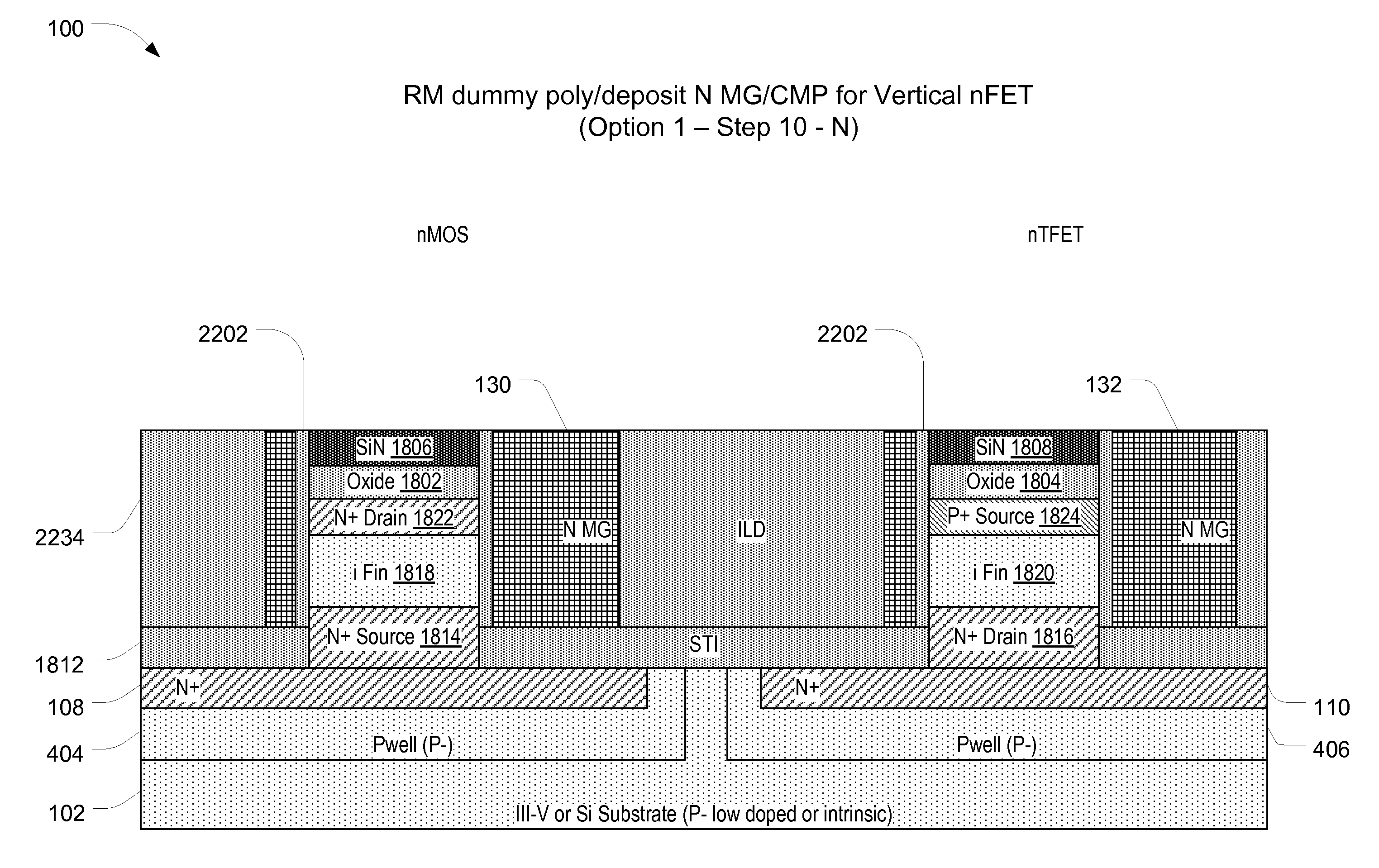
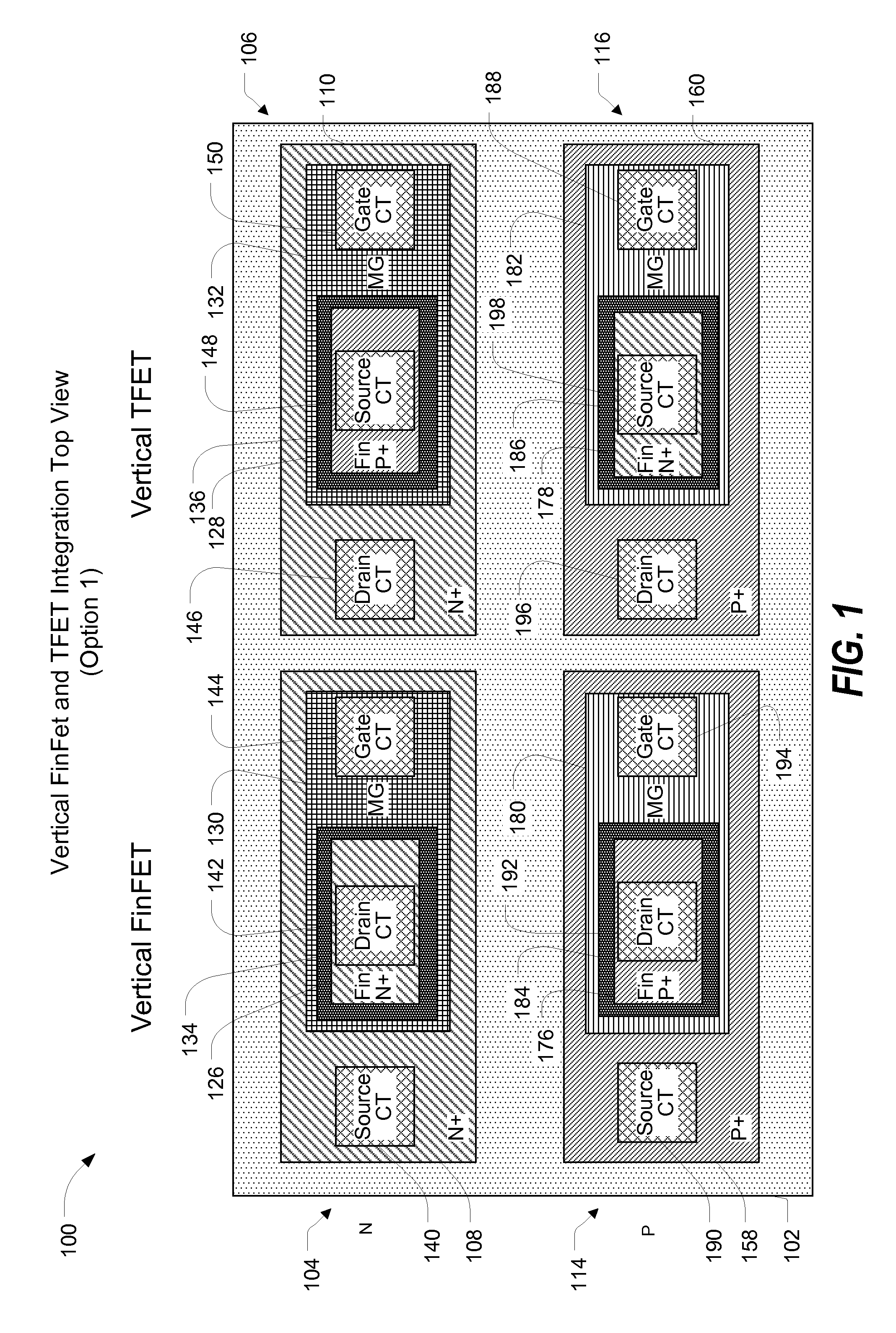
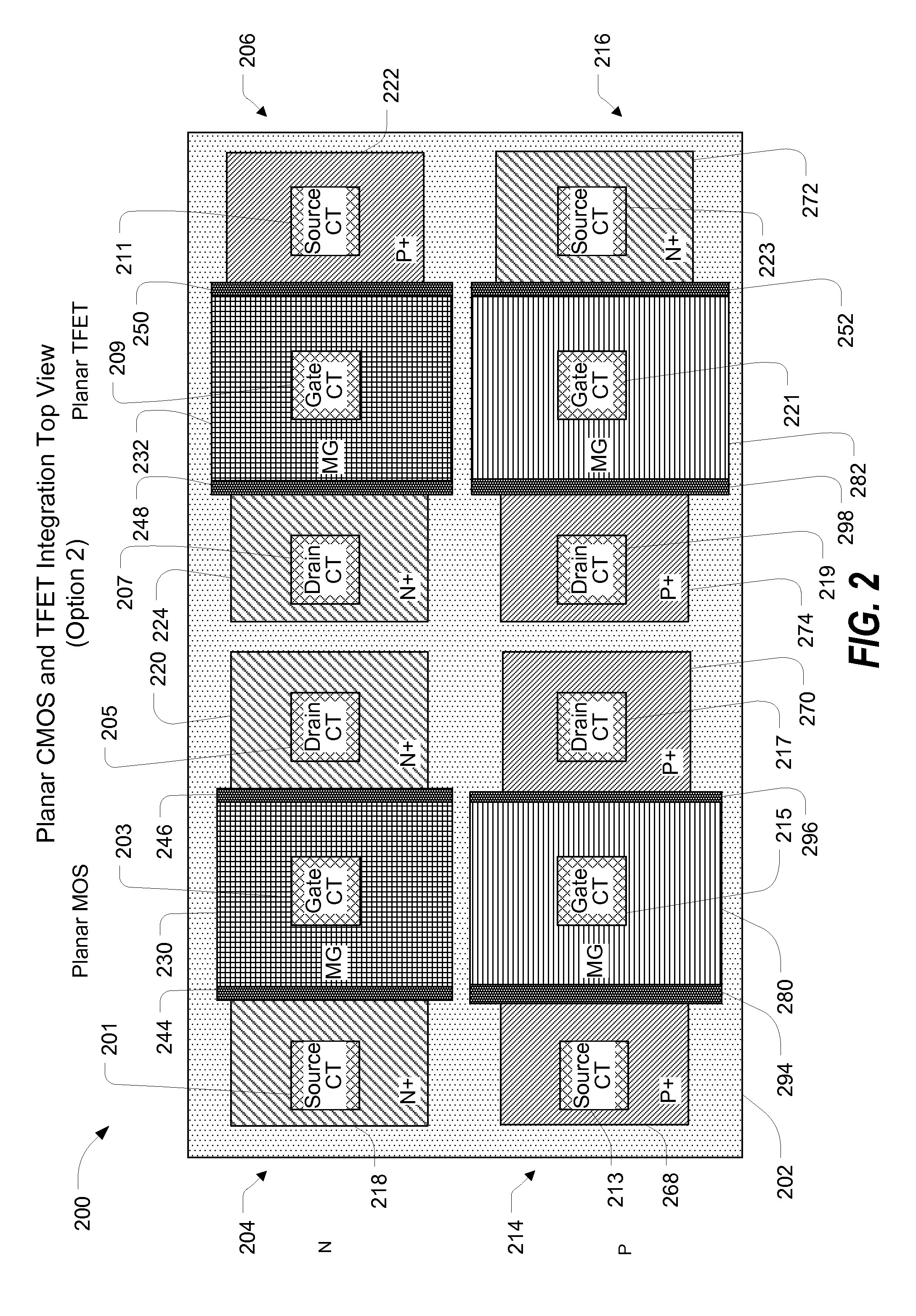
[0072]Referring to FIG. 1, an illustrative diagram of a top view of a structure as formed during at least one stage in a process of fabricating an electronic device is disclosed and generally designated 100. The structure 100 may correspond to a semiconductor device, an integrated circuit device, or another electronic device. The structure 100 includes a vertical CMOS transistor and a vertical TFET formed on a single substrate 102 (e.g., a III-V compound layer or a silicon (Si) layer). At least one of the vertical CMOS transistor or the vertical TFET may be configured to support a current flow direction between a source and drain that is perpendicular to the single substrate 102, as described herein. The CMOS transistor may include an n-type metal-oxide semiconductor transistor (nMOS) 104 and a p-type metal-oxide semiconductor transistor (pMOS) 114. The TFET may include an n-type TFET (nTFET) 106 and a p-type TFET (pTFET) 116. The nMOS 104 may correspond to an n-type fin-shaped fiel...


PUM


Abstract

An apparatus includes a structure that includes a single substrate, a planar complementary metal-oxide semiconductor (CMOS) transistor formed on the single substrate, a planar tunnel field-effect transistor (TFET) formed on the single substrate, and a mobility enhancement strength layer included in the planar CMOS transistor or included in the planar TFET.

Description

I. FIELD[0001]The present disclosure is generally related to complementary metal-oxide semiconductor (CMOS) transistor and tunnel field-effect transistor (TFET) on a single substrate.II. DESCRIPTION OF RELATED ART[0002]Advances in technology have resulted in smaller and more powerful personal computing devices. For example, there exist a variety of portable personal computing devices, including wireless computing devices, such as mobile phones, smart phones, netbooks, and laptops that are small, lightweight, and easily carried by users. More specifically, such devices may communicate voice and data packets over wireless networks. Many such devices incorporate additional features to provide enhanced functionality for end users. For example, a smart phone can also include a digital still camera, a digital video camera, a digital recorder, and an audio file player. Also, such devices can process executable instructions, including software applications, such as a web browser application...

Claims


Application Information

Patent Timeline
Patent Type & Authority Applications(United States)
IPC IPC(8): H01L27/088H01L29/161H01L21/02H01L29/78H01L21/8234H01L29/16H01L29/165
CPCH01L27/088H01L29/1608H01L29/161H01L29/165H01L29/7851H01L29/7827H01L21/823418H01L21/02529H01L21/02532H01L21/823487H01L29/7848H01L21/823814H01L27/0922H01L29/7391H01L27/092H01L29/66356H01L29/66545H01L29/6659H01L29/66628H01L29/66636H01L29/66666H01L29/0847
Inventor YANG, BINLI, XIAYUAN, JUN
Owner QUALCOMM INC
Why Eureka
Try Eureka