Semiconductor device

Active Publication Date: 2016-09-29
DENSO CORP
View PDF0 Cites 4 Cited by
  • Summary
  • Abstract
  • Description
  • Claims
  • Application Information

AI Technical Summary

Benefits of technology

The present teachings focus on improving the crack resistance of semiconductor devices. The technical effect of the present configuration is to reduce the likelihood of cracks forming and running into the electrode layer of the device. This is achieved by providing a crack starting point layer that allows for the safe generation of cracks and the formation of an alloy with the solder layer, which prevents the crack from running into the electrode layer.

Problems solved by technology

In a general semiconductor device, due to a temperature cycle in which a temperature of the semiconductor device repeatedly rises and falls during its use, there may be a case where a stress is exerted on an inside of the semiconductor device and a crack (cracking) occurs.

Method used


Image

  • Semiconductor device
  • Semiconductor device
  • Semiconductor device

Examples


Embodiment Construction

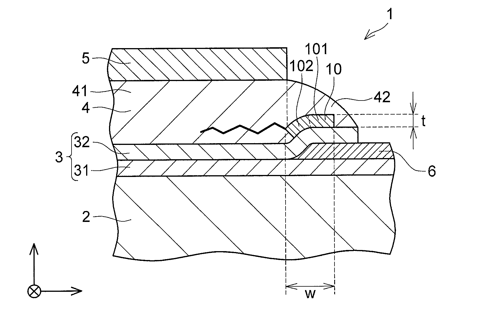
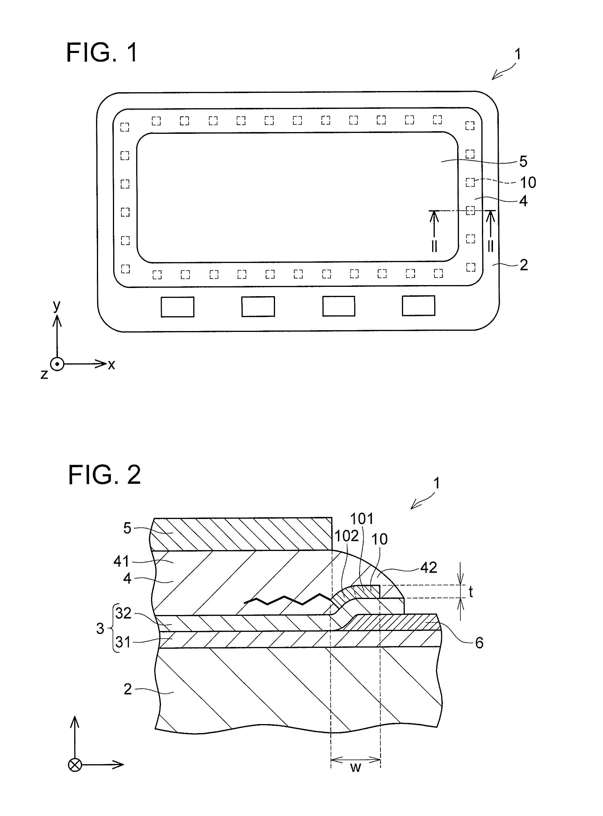
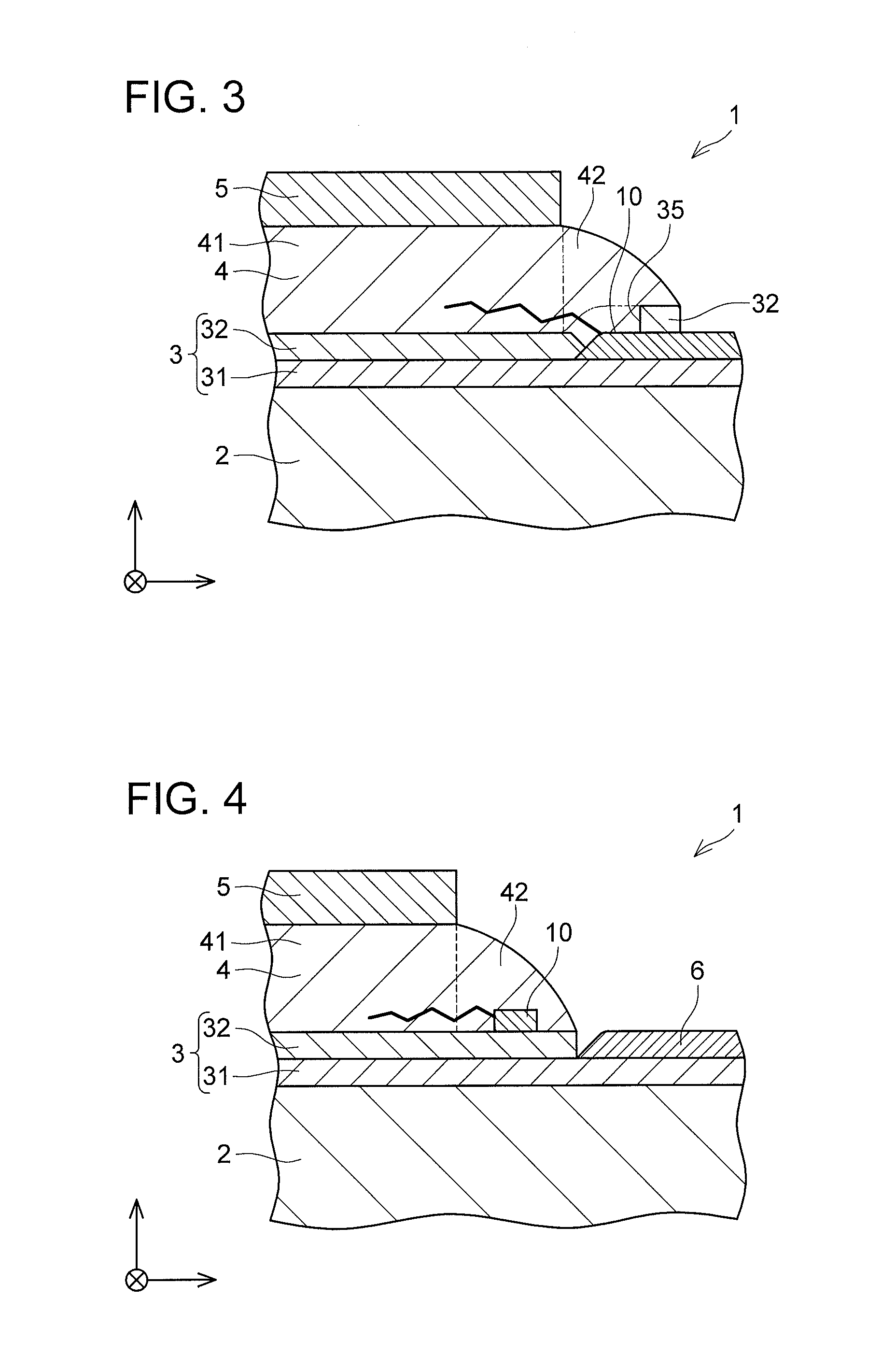
[0018]Embodiments will hereinafter be described with reference to the attached drawings. As shown in FIGS. 1 and 2, a semiconductor device 1 according to an embodiment comprises a semiconductor layer 2, an electrode layer 3 arranged on the semiconductor layer 2, crack starting point layers 10 arranged above the semiconductor layer 2, and a solder layer 4 being in contact with the electrode layer 3 and the crack starting point layers 10. The respective layers are stacked along a vertical direction (z direction). Notably, although the crack starting point layers 10 are covered with the solder layer 4 and hence cannot in actuality be seen in the plan view in FIG. 1, the crack starting point layers 10 are indicated by solid lines in FIG. 1 for description purpose.

[0019]The semiconductor layer 2 is configured such that regions of n-type or p-type are formed by implanting impurities into a semiconductor substrate made of silicon (Si), silicon carbide (SiC), or the like, for example. As th...


PUM


Abstract

A semiconductor device includes a semiconductor layer, an electrode layer arranged on the semiconductor layer, a crack starting point layer arranged above the semiconductor layer, and a solder layer being in contact with the electrode layer and the crack starting point layer. A joining force between the solder layer and the crack starting point layer is smaller than a joining force between the solder layer and the electrode layer.

Description

TECHNICAL FIELD[0001]The present teachings relate to a semiconductor device.BACKGROUND ART[0002]In a general semiconductor device, due to a temperature cycle in which a temperature of the semiconductor device repeatedly rises and falls during its use, there may be a case where a stress is exerted on an inside of the semiconductor device and a crack (cracking) occurs. Patent Literature 1 (Japanese Patent Application Publication No. 2011-023631) discloses an art for improving resistance to cracks that occur in a semiconductor device. A configuration disclosed in Patent Literature 1 includes a semiconductor element, and an electrode layer arranged to face the semiconductor element. Moreover, this configuration includes an intermediate joint layer and a solder joint layer on a surface of the semiconductor element that faces the electrode layer. Moreover, semiconductor element protection resin is provided in a coating manner on the semiconductor element, and at least in an outer peripher...

Claims


Application Information

Patent Timeline
IPC IPC(8): H01L23/00
CPCH01L24/29H01L2224/29076H01L2924/01013H01L2924/3512H01L2924/01006H01L2924/07025H01L2924/0483H01L23/3157H01L23/562H01L2924/0002H01L2224/29036H01L2224/26125H01L24/32H01L24/83H01L2224/02165H01L2224/04026H01L2224/05647H01L2224/05655H01L2224/29013H01L2224/29111H01L2224/32058H01L2224/83007H01L2224/83801H01L2224/05572H01L2224/32245H01L2924/13055H01L2924/13091H01L2924/01047H01L2924/01029H01L2924/00014H01L2924/00
Inventor FUKAMI, TAKESHI
Owner DENSO CORP
Why Eureka
Try Eureka