Microlens array, manufacturing method thereof, image acquisition device, and display device

Inactive Publication Date: 2016-10-13
BOE TECH GRP CO LTD
View PDF5 Cites 2 Cited by
  • Summary
  • Abstract
  • Description
  • Claims
  • Application Information

AI Technical Summary

Benefits of technology

The present invention provides a microlens array with improved precision and uniformity. The manufacturing process involves instilling a prepolymer into accommodation grooves of a microlens array and allowing the prepolymer to self-assemble to form curved protrusions that can maintain a stable shape after being cured. This process is convenient for manufacturing large-scale microlens arrays and reduces the cost by allowing the microlens array to be formed on a display panel.

Problems solved by technology

A traditional microlens array is mainly manufactured with a grinding tool or by machining, and the processing size and precision thereof is limited by the grinding tool and the machining equipment.
Meanwhile, a large-scale microlens array manufactured by using the existing process has the problem of poor precision and uniformity, and cannot meet the requirements for the integral imaging.

Method used


Image

  • Microlens array, manufacturing method thereof, image acquisition device, and display device
  • Microlens array, manufacturing method thereof, image acquisition device, and display device
  • Microlens array, manufacturing method thereof, image acquisition device, and display device

Examples


Embodiment Construction

[0045]Embodiments of the present invention will be described in detail below in conjunction with the drawings. In should be understood that, the embodiments set forth herein are merely for the purpose of describing and explaining the present invention, but not for limiting the present invention.

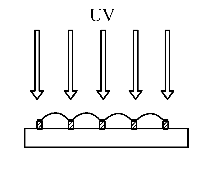
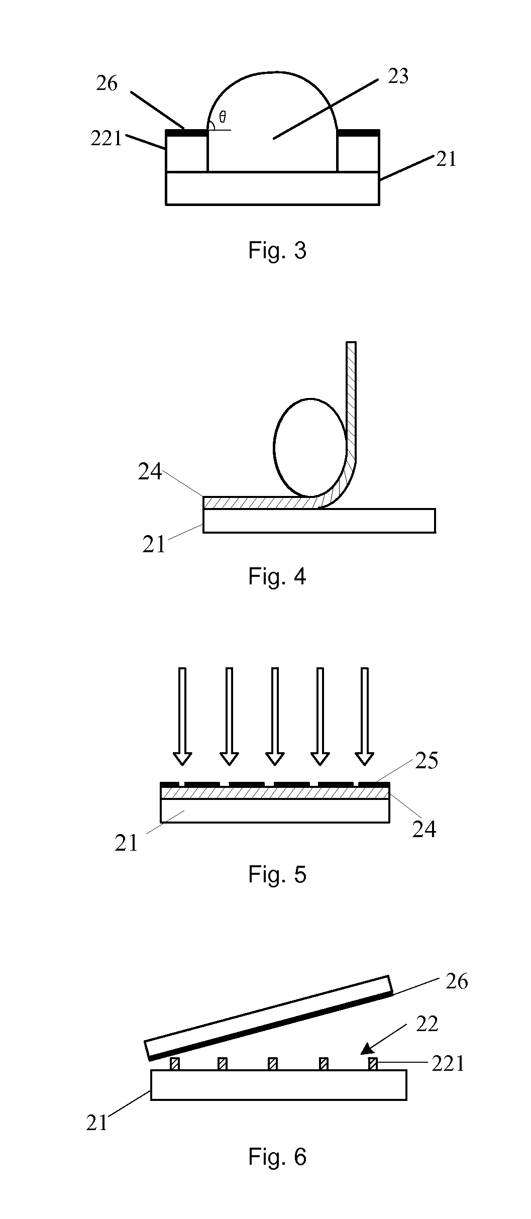
[0046]As an aspect of the present invention, there is provided a manufacturing method of a microlens array, which, as shown in FIG. 2, includes steps of:[0047]providing a substrate 21 (see step S1 in FIG. 2);[0048]forming a plurality of accommodation grooves 22 on the substrate 21 (see step S2 in FIG. 2);[0049]instilling a colloidal prepolymer 23 into each of the plurality of accommodation grooves 22, so that a top surface of the prepolymer 23 forms a curved surface protruding outwards, as shown in FIG. 7 (see step S3 in FIG. 2); and[0050]curing the prepolymer 23, so that the prepolymer 23 in each of the plurality of accommodation grooves is cured to form a microlens unit, thereby obtaining t...


PUM

PropertyMeasurementUnit
Viscosityaaaaaaaaaa
Lengthaaaaaaaaaa
Volumeaaaaaaaaaa

Abstract

The present invention provides a microlens array, a manufacturing method thereof, an image acquisition device, and a display device. The manufacturing method of a microlens array includes steps of: providing a substrate; forming a plurality of accommodation grooves on the substrate; instilling a colloidal prepolymer into each of the plurality of accommodation grooves, so that a top surface of the prepolymer forms a curved surface protruding outwards; and curing the prepolymer, so that the prepolymer in each of the plurality of accommodation groove is cured to form a microlens unit, thereby obtaining the microlens array. The manufacturing method provided by the present invention is simple, is applicable to a large-scale microlens array, and the manufactured microlens array has better precision and uniformity.

Description

FIELD OF THE INVENTION[0001]The present invention relates to the field of integral imaging technology, and in particular, relates to a microlens array, a manufacturing method thereof, an image acquisition device, and a display device.BACKGROUND OF THE INVENTION[0002]New display technologies are continuously developed along with the advent of the concept of 3D display, and an integral imaging technology is a display technology which reproduces the light field of an object in a space or images an object within a certain spatial range. The integral imaging technology is an all-true 3D stereoscopic display technology and free of conflict between the display principle thereof and the principle of human vision, will not cause the stereoscopic viewing fatigue as before and can perform omnidirectional three-dimensional display, and thus becomes a next generation display technology which attracts increasing attention.[0003]As shown in FIG. 1, an integral imaging technology based on a microle...

Claims


Application Information

Patent Timeline
IPC IPC(8): G02B3/00B29D11/00G02B27/22
CPCG02B3/0018G02B27/2214B29K2995/0031B29D11/0048B29D11/00442B29D11/00375G02B3/0006G02B3/0012G02B30/27B29D11/00298G03F7/0005G03F7/027G03F7/038
Inventor ZHOU, CHUNMIAO
Owner BOE TECH GRP CO LTD
Why Eureka
Try Eureka