Pixel structure, mask plate and display device

A pixel structure and display device technology, applied in vacuum evaporation plating, coating, electric solid devices, etc., can solve the problems of difficulty in ensuring sub-pixel aperture ratio, affecting product life, brightness, and difficulty in realizing high resolution, etc., to achieve Improve the effect of evaporation, prevent deformation, and reduce the difficulty of manufacturing process

Inactive Publication Date: 2018-07-24
BOE TECH GRP CO LTD +1
View PDF3 Cites 15 Cited by
  • Summary
  • Abstract
  • Description
  • Claims
  • Application Information

AI Technical Summary

Problems solved by technology

Among them, FMM generally has the limitation of the minimum opening, and the sub-pixels of different colors in the evaporation process are limited by the opening pitch. Therefore, the preparation of AMOLED is inevitably limited by the FMM opening and the precision of the evaporation process. It is difficult to achieve high resolution. If a higher resolution is required, it is difficult to ensure the aperture ratio of the sub-pixels, making it difficult to achieve high resolution, and even affect the product's lifespan, brightness and other characteristics

Method used


Image

  • Pixel structure, mask plate and display device
  • Pixel structure, mask plate and display device
  • Pixel structure, mask plate and display device

Examples


Embodiment 1

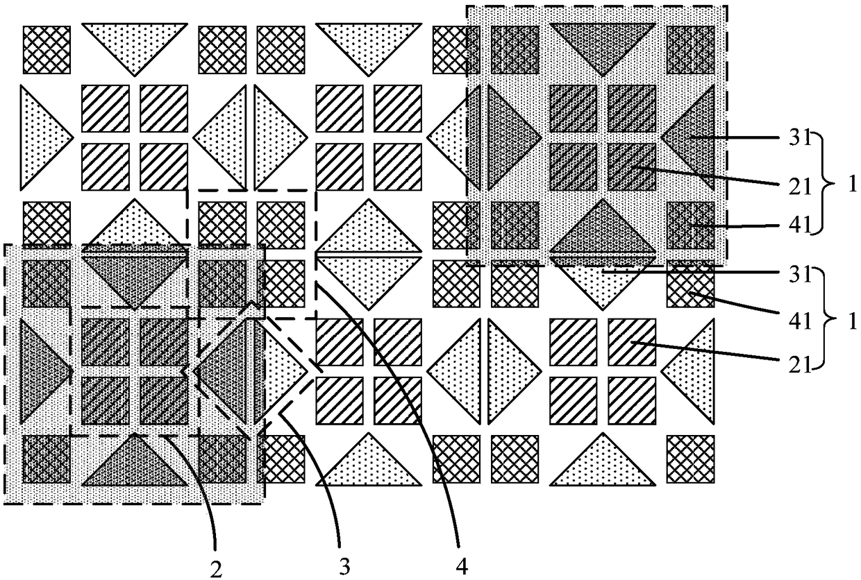
[0027] This embodiment provides a pixel structure, including: a plurality of repeating units arranged in an array (such as figure 1 shown in the shaded part), the outer contour of each repeating unit is a rectangle, which includes four first sub-pixels 21, four second sub-pixels 31 and four third sub-pixels 41, wherein the four first sub-pixels The pixels 21 are arranged in the center of the repeating unit in a 2×2 array, forming the first sub-pixel group 2; the four second sub-pixels 31 are respectively located on the four sides of the repeating unit; the four third sub-pixels 41 are respectively located on the four sides of the repeating unit. vertex angle; in any two adjacent repeating units, two adjacent second sub-pixels 31 form a second sub-pixel group 3, and the outer contour of the second sub-pixel group 3 is a polygon or a circle; any four are in the form of a polygon Among the four repeating units arranged in a 2×2 array, four adjacent third sub-pixels 41 form a thir...

Embodiment 2

[0038] This embodiment provides a display device including any one of the pixel structures provided in Embodiment 1.

[0039]The display device can be any product or component with a display function such as a liquid crystal panel, an electronic paper, an OLED panel, a mobile phone, a tablet computer, a television, a monitor, a notebook computer, a digital photo frame, a navigator, and the like.

[0040] Preferably, the display device is an organic light-emitting diode (OLED; Organic Light-Emitting Diode;) display device. In the display device, since the pixel structure has a better evaporation process effect, the product yield of the display device is higher; moreover, since the mask opening for preparing the pixel structure is relatively large, the aperture ratio is improved, and the light emitting area is increased. Large, so as to improve the product brightness, lifespan and image quality definition of the organic light-emitting diode (OLED; Organic Light-Emitting Diode;) ...

Embodiment 3

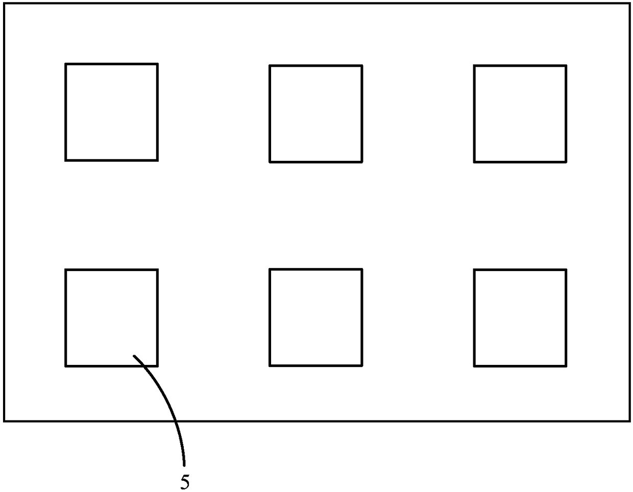
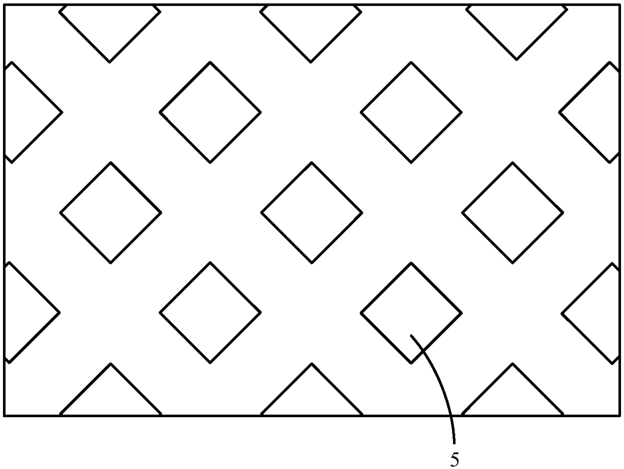
[0042] like Figure 2 to Figure 4 As shown, this embodiment provides a mask for preparing any one of the pixel structures provided in Embodiment 1.

[0043] The mask plate includes: a substrate, and a mask opening 5 on the substrate corresponding to the outline of the sub-pixel group.

[0044] Compared with the mask plate in the prior art, the mask opening 5 in the mask plate provided in this embodiment corresponds to the sub-pixel group in the pixel structure provided in Embodiment 1, that is, the mask in this embodiment The opening 5 corresponds to four sub-pixels of the same color. Specifically, the first sub-pixel group, the second sub-pixel group and the third sub-pixel group can be respectively prepared by using three kinds of masks with different openings, for example, using figure 2 The mask plate shown is used to prepare the first sub-pixel group, using image 3 The mask plate shown is used to prepare the second sub-pixel group, using Figure 4 The mask plate sho...


PUM


Abstract

The invention provides a pixel structure, a mask plate and a display device, which belongs to the field of display technologies and can solve a problem that the aperture ratio of sub-pixels is limitedby a mask opening of the existing mask plate. The pixel structure comprises a plurality of repeating units which are arranged in an array mode, wherein each repeating unit is rectangular in outer contour and comprises four first sub-pixels, four second sub-pixels and four third sub-pixels, the four first sub-pixels are arranged at the center of the repeating unit in a 2*2 array mode to form a first sub-pixel group; the four second sub-pixels are respectively located at four sides of the repeating unit; the four third sub-pixels unit are respectively located at four top corners of the repeating unit; two adjacent second sub-pixels in any two adjacent repeating units form a second sub-pixel group, and the second sub-pixel group is polygonal or circular in outer contour; and four adjacent third sub-pixels in any four repeating units arranged in the 2*2 array mode form a third sub-pixel group.

Description

technical field [0001] The invention belongs to the field of display technology, and in particular relates to a pixel structure, a mask plate and a display device. Background technique [0002] Commonly used flat panel display devices generally include LCD (Liquid Crystal Display: Liquid Crystal Display) and OLED (Organic Light-Emitting Diode: Organic Light-Emitting Diode) display devices. In particular, OLED display devices have many advantages such as self-luminescence, fast response speed, and wide viewing angle compared with LCDs, and are suitable for various applications such as flexible displays, transparent displays, and 3D displays. [0003] At present, in the preparation process of top-emitting active matrix organic light-emitting diode (AMOLED) panels, a high-precision metal mask (Fine Metal Mask, FMM for short) is usually used to form an organic light-emitting layer by evaporation through an evaporation process. Among them, FMM is generally limited by the minimum...

Claims


Application Information

Patent Timeline
Patent Type & Authority Applications(China)
IPC IPC(8): H01L27/32H01L51/56C23C14/04
CPCC23C14/042H10K59/353H10K71/166
Inventor 王志强
Owner BOE TECH GRP CO LTD
Why Eureka
Try Eureka