Advanced PCI Express Board Assembly

a technology of pci express and assembly, which is applied in the field of high-performance computer technology, can solve the problems of limiting the possibility of using the bottom side of the pci express limiting the possibility of using the to surface of the daughter board for high electronic components or wireless modules, and limiting the air flow between the daughter board and the pci express add-in board. , to achieve the effect of preventing pcb from twis

Active Publication Date: 2016-10-13
FELDMAN MICHAEL +1
View PDF3 Cites 5 Cited by
  • Summary
  • Abstract
  • Description
  • Claims
  • Application Information

AI Technical Summary

Benefits of technology

[0015]The first aspect of the present invention consists in that the offered Advanced PCI Express board assembly allows significantly increasing the number of high electronic components or modules of height up to 8.57 mm compare to traditional PCI Express add-in board.
[0017]The third aspect of the present invention consists in that the offered assembly increases an efficiency of the air flow cooling by allowing placing high components or modules on both sides of the PCB.
[0018]The fourth aspect of the present invention consists in that said assembly represents wide opportunity of using exchangeable male edge PCI Express connectors corresponding to x1, x2, x4, x8 or x16 lanes. This architecture allows plugging proposed PCI Express assembly in to different motherboard female PCI Express connectors.
[0019]The next aspect consists in that there is no restriction for the thickness of the PCB on which a high components are placed, because this PCB not intend to be plugged into PCI Express female connector. The thickness of this PCB can be increased to prevent PCB twisting because of the PCB length and heavily components installation.

Problems solved by technology

These requirements essentially limit the possibility of using the bottom side of the PCI Express board for high electronic components or wireless modules placement.
Therefore, the height of said components that are located between top surface of the PCI Express add-in board and bottom surface of the daughter board and height of the components on the to surface of the daughter board are significantly limited.
First, the air flow between daughter boards and PCI Express add-in board is limited, and the placement of electrical components that can generate significant amount of heat between daughter board and PCI Express add-in board (top side) is not possible.
Second, the tradition PCI Express add-in board with daughter board on the top side can't utilize the 2.67 mm. space on the bottom side of the PCI Express add-in board for high electronic components or modules placement (like transformers, relays, capacitors etc.).
Third disadvantage consists in that by using any additional daughter board the maximum height of the electronic components that can be located on the top side of the PCI Express board is reduced by the value equal to the daughter board thickness.
That makes impossible to install electronic components with the height more than 4 mm.
Fourth disadvantage is that all known standard solutions with daughter boards cannot be used for the placement of multiple replaceable modules (for example wireless modules in MiniPCI Express or M.2 form factor that can have height more than 6 mm.).
But even if the modules are placed between daughter board and PCI Express add-in board, they will become not accessible for replacement.

Method used


Image

  • Advanced PCI Express Board Assembly
  • Advanced PCI Express Board Assembly
  • Advanced PCI Express Board Assembly

Examples


Embodiment Construction

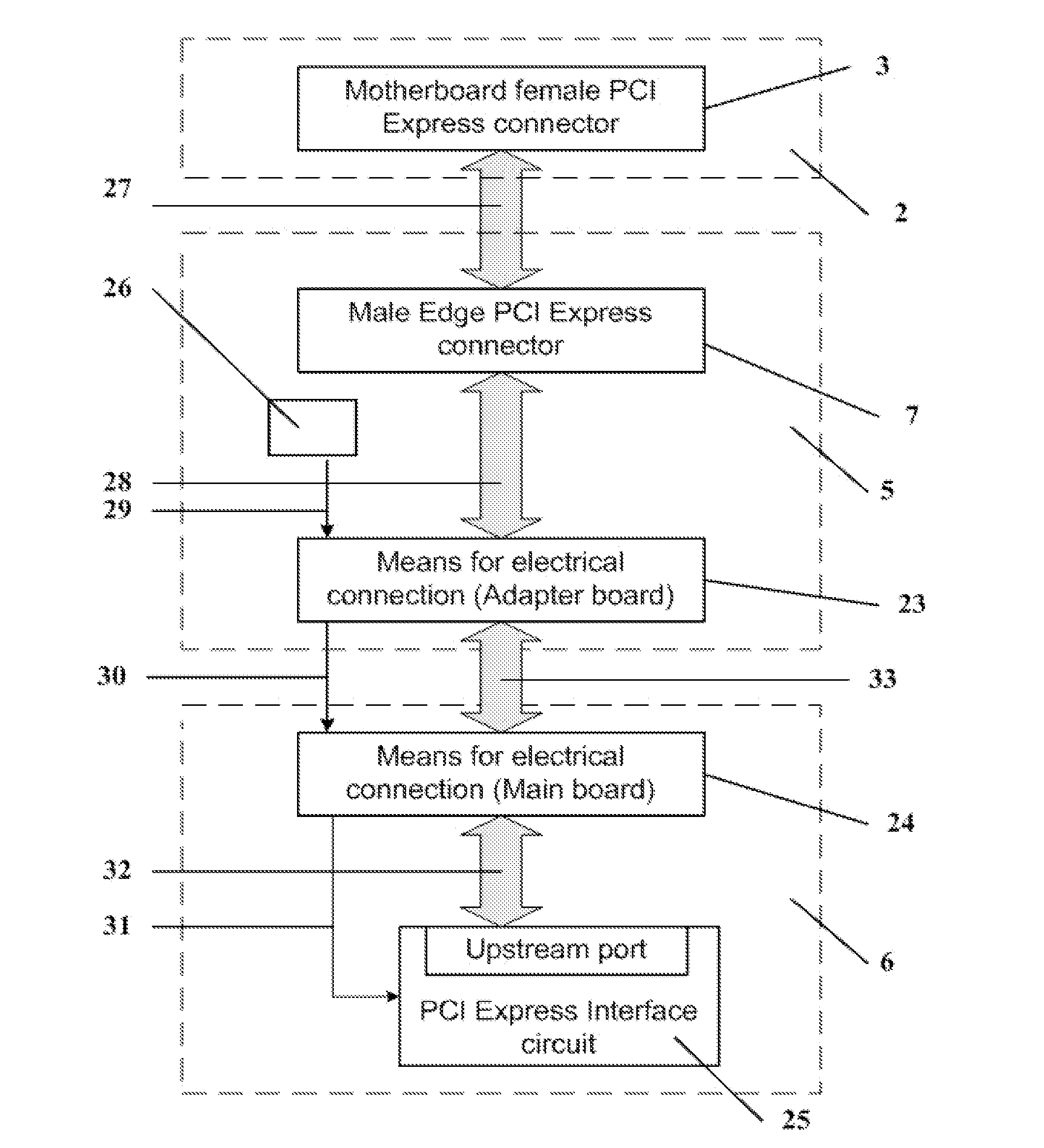
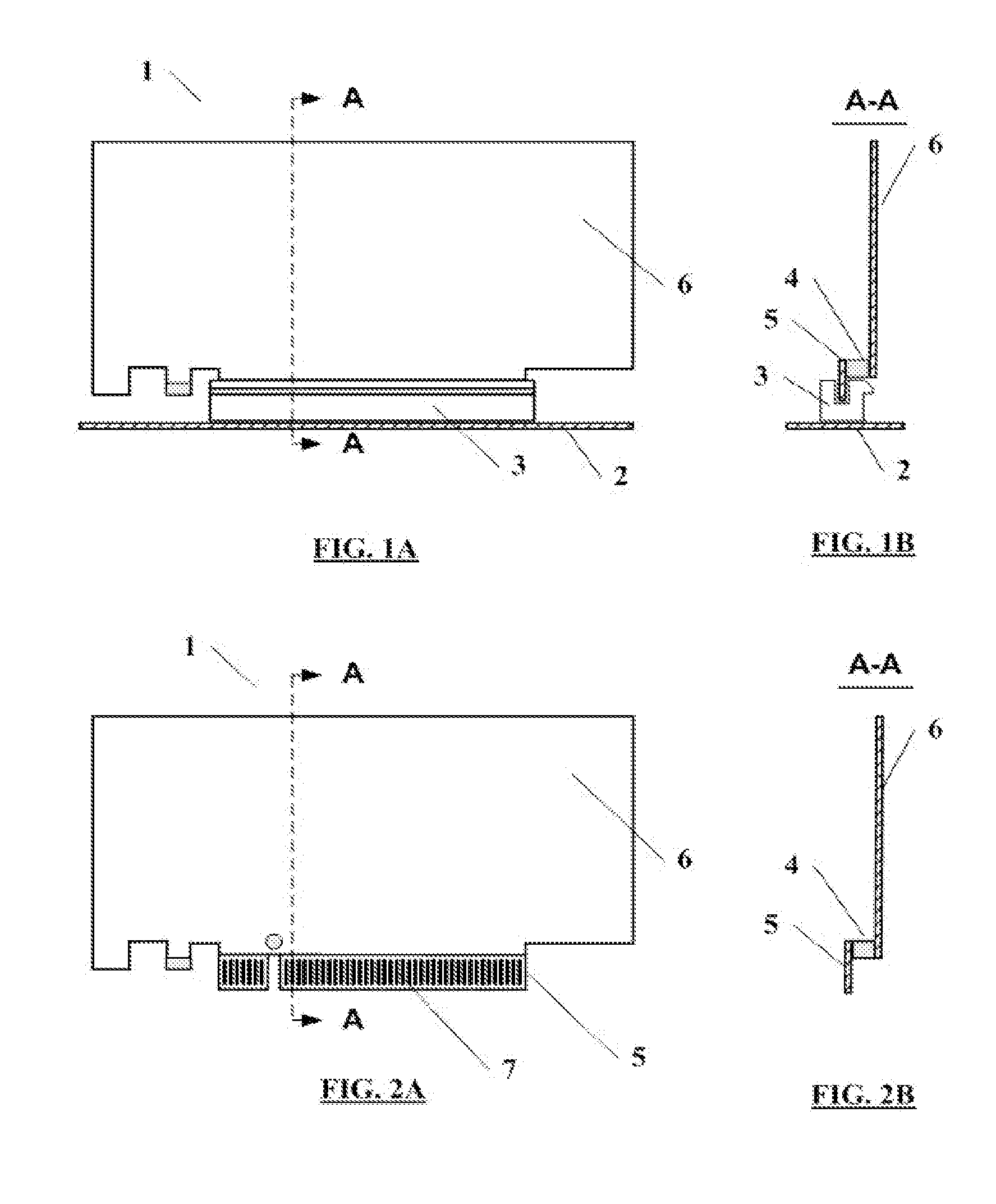
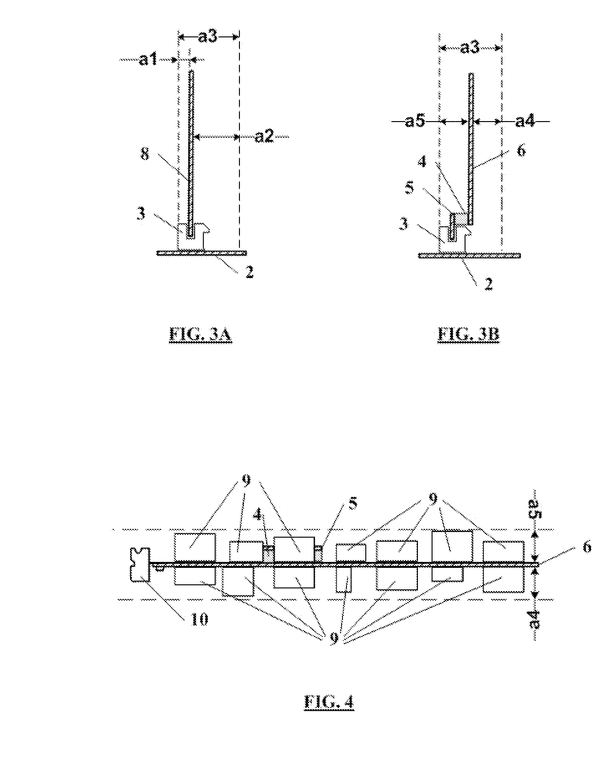
[0028]FIG. 1A represents a view of the proposed Advanced PCI Express board assembly 1 inserted into female PCI Express connector 3 that is located on a computer system board 2, for example, a motherboard. The proposed Advanced PCI Express board assembly (FIG. 1B) consists of the Main board 6, the Adapter board 5 and means for electrical and mechanical connection 4 of said Main board 6 and Adapter board 5. For electrical connection of said Adapter board 5 and Main board 6 can be used one or more connectors. For additional mechanical stabilization can be used spacers, that can be fixed on the Adapter and / or Main board via solder, glue, screws etc. The connection between said Adapter board and said Main board can be permanent when there is no possibility to disconnect both boards after assembly or, on the contrary, both boards can be disconnected after assembly.

[0029]FIG. 2A represents a top side view of the Advanced PCI Express board assembly wherein the male edge PCI Express connecto...


PUM


Abstract

An advanced PCI Express board assembly is intended for efficiently placing more electronic components or modules having a large height (up to 8.57 mm) in comparison with traditional PCI Express add-in boards. This assembly comprises two PCBs connected together. The first one has the minimum possible sizes. This PCB includes a PCI Express male edge connector and is intended to be plugged in to motherboard female PCI Express connector. The second PCB is parallel to first one and is located in the middle of the space (slot) defined for one add-in PCI Express board. This position makes possible to place high electronic components or modules on the both sides (top and bottom) of the second PCB.

Description

CROSS-REFERENCE TO RELATED APPLICATION[0001]This is the first application filed for the present invention.TECHNICAL FIELD[0002]The present invention relates to the field of high-performance computer technology and, in particular, to add-in PCI Express Boards intended for a compact arrangement the large numbers of high electronic components or modules.BACKGROUND[0003]Today there is a class of the PCI Express boards that dedicated for the multichannel wireless communication market. The main feature of these boards is that these boards are using different wireless modules or blocks located on the PCB surface. The most of these wireless modules are implemented in a MiniPCI Express or M.2 form factor.[0004]The wireless modules itself or wireless modules in MiniPCI Express or M.2 form factor are significantly higher than any standard electronic components that can be placed on the PCI Express board PCB.[0005]The PCI Express add-in board specification limits the height of the components th...

Claims


Application Information

Patent Timeline
Patent Type & Authority Applications(United States)
IPC IPC(8): G06F13/40G06F13/42G06F13/362
CPCG06F13/409G06F13/4282G06F13/4068G06F13/362G06F13/4022G06F13/4295G06F2213/0026
Inventor FELDMAN, MICHAELFELDMAN, BORIS
Owner FELDMAN MICHAEL
Why Eureka
Try Eureka