Laminated composite electronic device including coil and capacitor

a technology of laminated composite electronic devices and capacitors, which is applied in the direction of multiple-port network, electrical apparatus, structure fixed capacitor combinations, etc., can solve the problems of difficult simultaneous providing a high performance and a reduction in size and height, difficult to ensure a sufficient space, and reducing q-value and inductance value, so as to improve the character of the coil

Active Publication Date: 2016-10-20
TDK CORPARATION
View PDF0 Cites 17 Cited by
  • Summary
  • Abstract
  • Description
  • Claims
  • Application Information

AI Technical Summary

Benefits of technology

[0012]On the other hand, the requirement for simultaneous accomplishment of such improved characteristics with the reduction in size and height is thought to be increased more and more in the future in step with the trend of pursuing a reduction in size and height, more functions, and higher functions for electronic equipment.
[0013]It is therefore an object of the present invention to provide a novel device structure for improving the characteristic of a coil in a laminated composite electronic device including a coil and a capacitor.
[0015]In the laminated composite electronic device of the present invention, instead of arranging a coil and a capacitor side by side as in the aforementioned conventional structure (FIGS. 17 and 18), the capacitor electrodes are arranged such that they lap over the coil conductors within an area in which the coil is arranged (see FIGS. 1 through 5 later described), so that the present invention can save the area which would otherwise be required to arrange the capacitor, and can correspondingly increase the diameter of the coil to achieve a high inductance value. Additionally, the coil conductor can be increased in line width, thereby achieving a high Q-value. Furthermore, a chip can be reduced in size (reduction in size when viewed from the vertical direction). For clarity, in this application, a description will be made with a term “vertical direction” referring to a direction in which layers are laminated in a laminate, and a term “horizontal direction” referring to a direction parallel to each conductor layer and insulating layer.
[0016]Also, in the present invention, a coil conductor which forms part of the coil also serves as one of a pair of electrodes (capacitor electrodes) which form a capacitor. Since the capacitor electrodes are arranged to oppose this coil conductor in the vertical direction, it is possible to prevent the flux of the coil from being blocked by the capacitor electrodes.
[0023]While a coil conductor generally draws an L-like or U-like (C-like) pattern within a conductor layer, when a capacitor electrode is made to have an L-like or U-like (C-like) plane shape so as to extend along the coil conductor in such a shape, the coil conductor can be effectively utilized as a capacitor electrode to ensure a wide electrode area for a capacitor and achieve a sufficient capacitance.
[0026]According to the present invention, the characteristic of a coil can be improved in a laminated composite electronic device including a coil and a capacitor.

Problems solved by technology

However, a reduction in size and height of a device may result in difficulties in ensuring a sufficient space for mounting each circuit element.
As such, it is not easy to simultaneously provide a high performance and a reduction in size and height.
For example, a reduction of a laminated low pass filter in size and height will inevitably result in a smaller diameter of a coil and a consequently lowering Q-value and inductance value, thus encountering difficulties in improving the performance.
As shown in these figures, when the coil L and capacitor C are disposed side by side in the horizontal direction, the coil L is reduced in diameter, and moreover, the capacitor C disposed adjacent to the coil L prevents flux F of the coil L from passing, possibly resulting in degraded characteristics of the coil L and inability to sufficiently satisfy required characteristics.

Method used


Image

  • Laminated composite electronic device including coil and capacitor
  • Laminated composite electronic device including coil and capacitor
  • Laminated composite electronic device including coil and capacitor

Examples


first embodiment

[0047]First, characteristic features of the present invention will be described as a first embodiment.

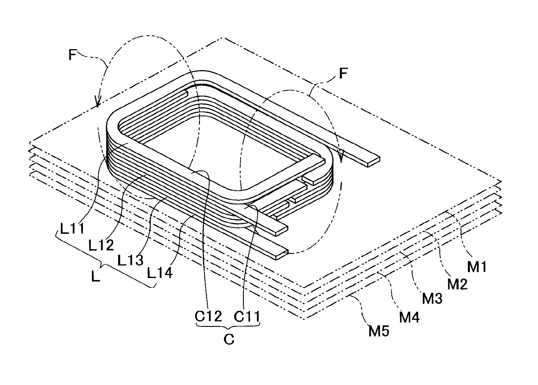
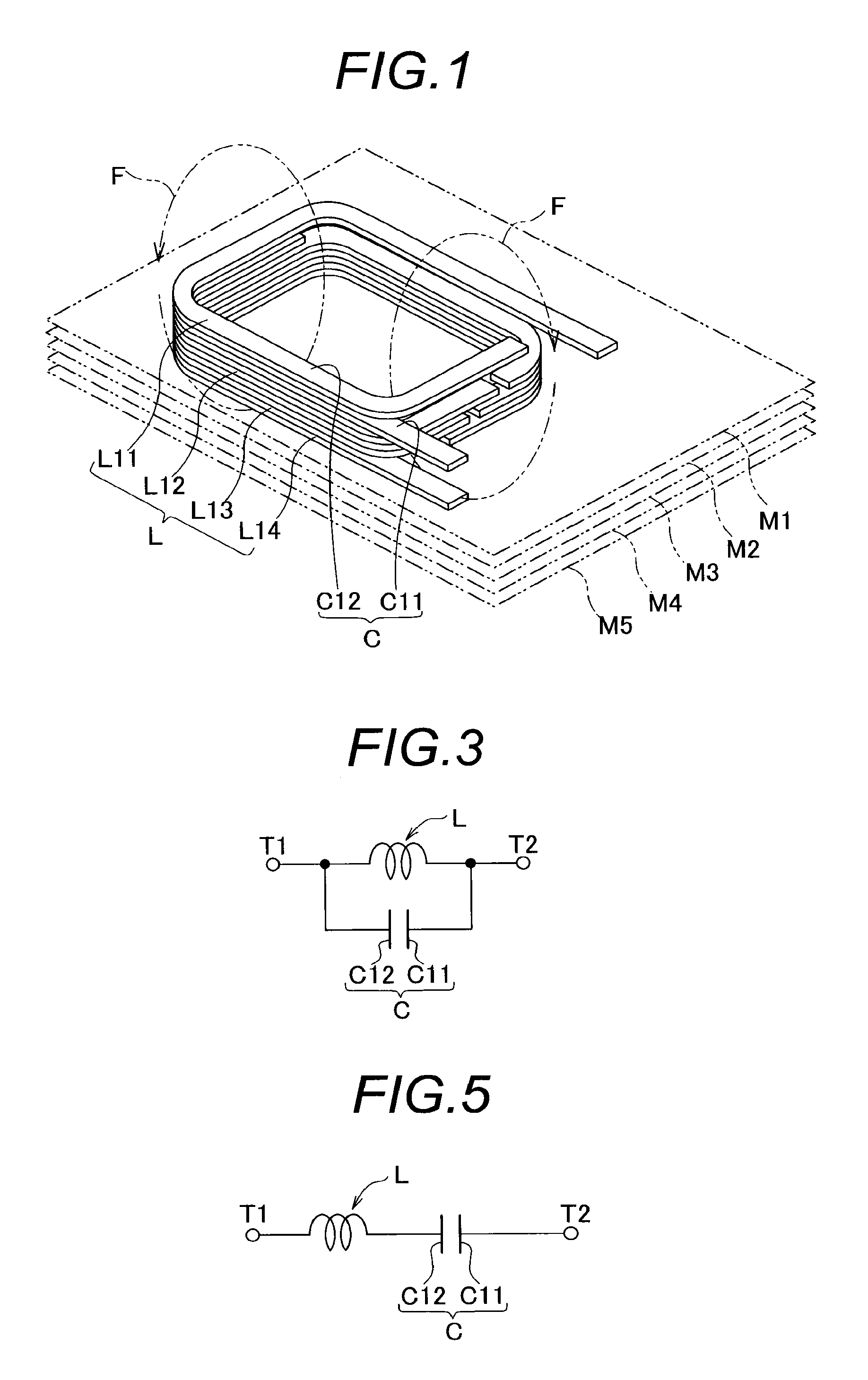
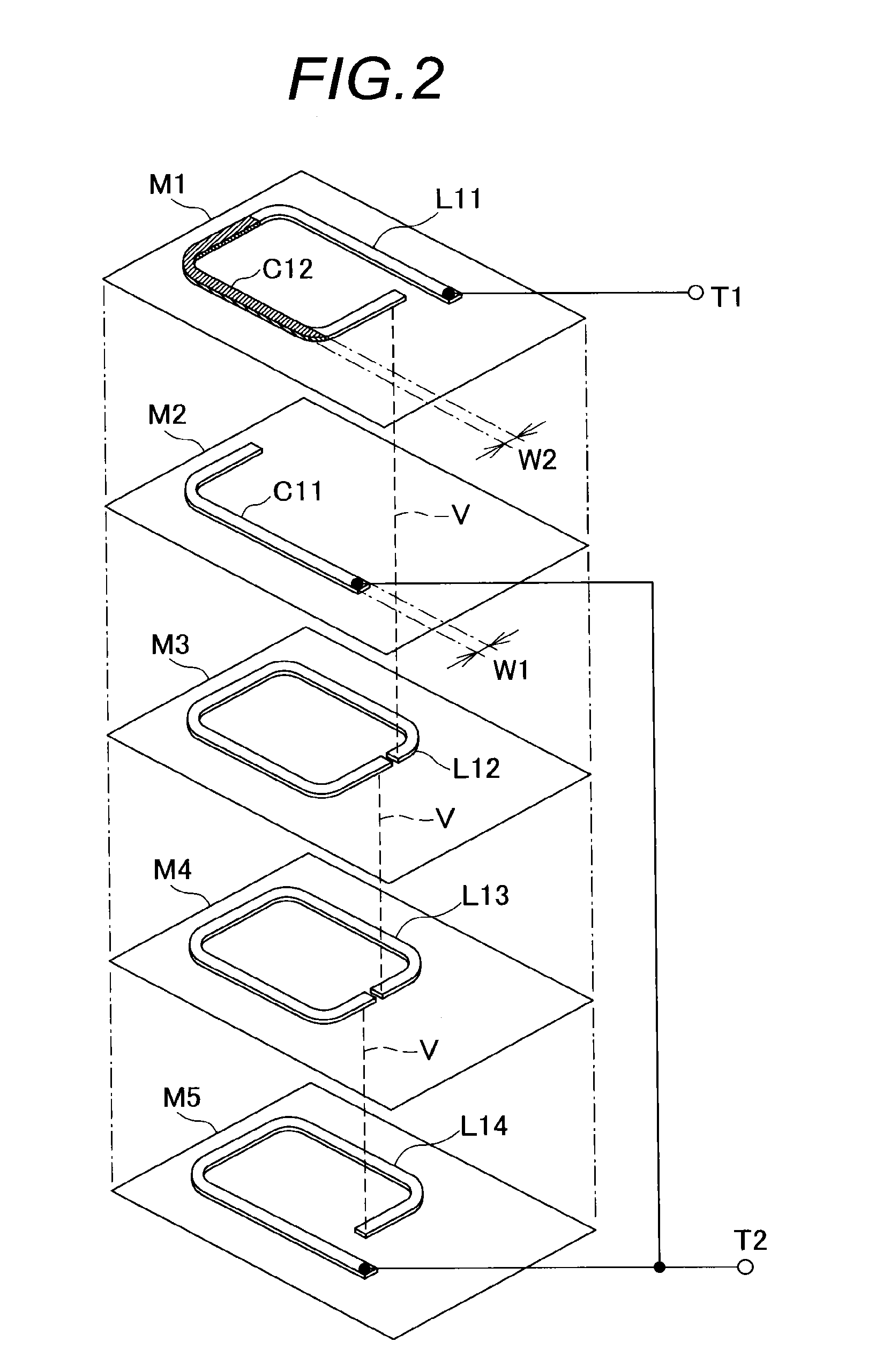
[0048]FIGS. 1-3 illustrate characteristic features in a laminated composite electronic device according to the present invention. As shown in these figures, the aforementioned convention structure (FIGS. 17 and 18) comprises a coil L and a capacitor C disposed side by side (horizontally), while the embodiment of the present invention comprises a capacitor C between coil conductors L11, L12 which together form a laminated coil L by inserting a capacitor electrode C11 between the coil conductors L11, L12, and arranging the capacitor electrode C11 such that it laps vertically over the coil conductor L11.

[0049]Specifically, a laminate is made up of five conductor layers including a first conductor layer M1 through a fifth conductor layer M5 which are laminated with an insulating layer (not shown) inserted between the respective conductor layers M1-M5. Loop-shaped coil conductors L11, L1...

second embodiment

[0058]A laminated composite electronic device according to a second embodiment of the present invention will now be described with reference to FIGS. 10 through 13.

[0059]A laminated composite electronic device 11 according to the second embodiment of the present invention is a laminated low-pass filter (hereinafter called the “LPF”) circuit, implemented in a chip, which comprises an LC filter made up of conductor patterns within a laminate including a plurality of conductor layers laminated with an insulating layer interposed between the respective conductor layers.

[0060]Specifically, as shown in FIG. 10, the circuit comprises two LC parallel circuits (a first LC resonant circuit made up of a coil L1 and capacitor C2 connected in parallel with each other, and a second LC resonant circuit made up of a coil L2 and a capacitor C4 connected in parallel with each other) connected in series between an input terminal T1 and an output terminal T2; a capacitor C1 having one end connected bet...

third embodiment

[0073]A laminated LPF according to a third embodiment of the present invention will be described with reference to FIG. 14.

[0074]As shown in FIG. 14, the LPF of this embodiment, like the second embodiment, employs coil-integrated capacitors for a capacitor C2 of a first LC resonant circuit and a capacitor C4 of a second LC resonant circuit, and in addition to these, employs coil-integrated capacitors for a capacitor C1 and a capacitor C5 as well.

[0075]Specifically, like the second embodiment, a coil conductor L11 forming part of a coil L1 of the first LC resonant circuit, and a coil conductor L21 forming part of a coil L2 of the second LC resonant circuit are arranged on a first conductor layer M1. In this structure, a capacitor electrode C11 of a capacitor C1 and a capacitor electrode C21 of a capacitor C2 are arranged on a second conductor layer M2 so as to oppose the coil conductor L11 of the first LC resonant circuit, thereby forming the capacitor C1 between the capacitor electr...


PUM


Abstract

A laminated composite electronic device has a circuit including a coil and a capacitor within a laminate having a plurality of conductor layers laminated with an insulating layer interposed between the respective ones of the conductor layers. The device includes a coil conductor arranged on a first conductor layer and forming part of the coil, and a pair of capacitor electrodes for forming the capacitor, one of which is arranged on a second conductor layer such that the one capacitor electrode laps over the coil conductor when viewed from a laminating direction of the laminate, wherein the coil conductor forms part of the coil, and simultaneously serves as the other of the pair of capacitor electrode for forming part of the capacitor.

Description

BACKGROUND OF THE INVENTION[0001]The present invention relates to a laminated composite electronic device including a coil and a capacitor, and more particularly, to a composite electronic device which comprises a circuit including a coil and a capacitor within a laminate.[0002]To respond to a demand for high-density mounting, composite electronic devices are nowadays provided by containing a plurality of passive elements within a single laminate chip to implement a variety of functions.[0003]For example, a laminated filter comprises a filter circuit composed of a coil and a capacitor within a laminate having a plurality of conductor layers laminated with an insulating layer interposed between the respective conductor layers, thereby allowing for accomplishing such functions as signal processing, EMC countermeasures, and the like. The laminated filter is widely employed in a variety of electronic equipment such as a mobile telephone, a smart phone, a personal computer, and the like....

Claims


Application Information

Patent Timeline
Patent Type & Authority Applications(United States)
IPC IPC(8): H03H7/01H01G4/40
CPCH03H7/0115H01G4/40
Inventor TANAKA, MASAMICHIITO, TOMOKAZU
Owner TDK CORPARATION
Why Eureka
Try Eureka