
Process chamber and semiconductor processing apparatus

Active Publication Date: 2016-11-03
BEIJING NAURA MICROELECTRONICS EQUIP CO LTD
View PDF5 Cites 3 Cited by
  • Summary
  • Abstract
  • Description
  • Claims
  • Application Information

AI Technical Summary

Benefits of technology

The invention is designed to improve the speed, accuracy, and uniformity of processing gases in semiconductor processing. This is achieved by improving the process chamber and the semiconductor processing apparatus.

Problems solved by technology

First, since the processing gas gradually diffuses from one side of the cavity 106 to the interior of the reaction chamber 118, the processing gas diffuses to the processing space at a low speed, and also, inside the reaction chamber 118, a distribution density of the processing gas within a region close to the gas inlet is inevitably higher than that within a region away from the gas inlet, so the distribution of the processing gas is nonuniform inside the reaction chamber 118, thereby adversely affecting the uniformity of process, and
Second, since not all the processing gas entering the cavity 106 can diffuse into the reaction chamber 118 and be involved in the processing, it is very hard to control a flow of the processing gas involved in the processing, thereby adversely affecting the processing results.

Method used


Image

  • Process chamber and semiconductor processing apparatus
  • Process chamber and semiconductor processing apparatus
  • Process chamber and semiconductor processing apparatus

Examples


Embodiment Construction

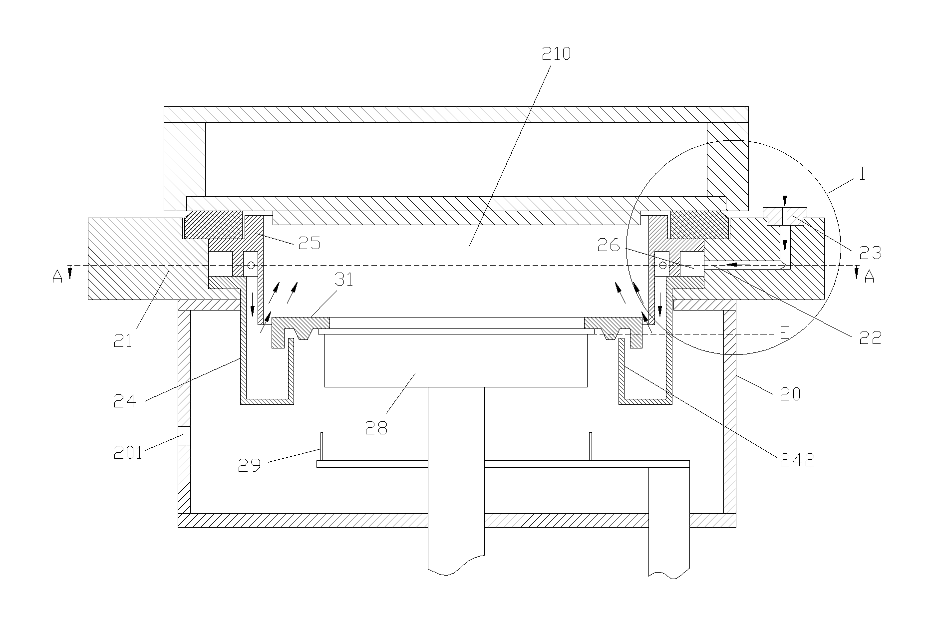
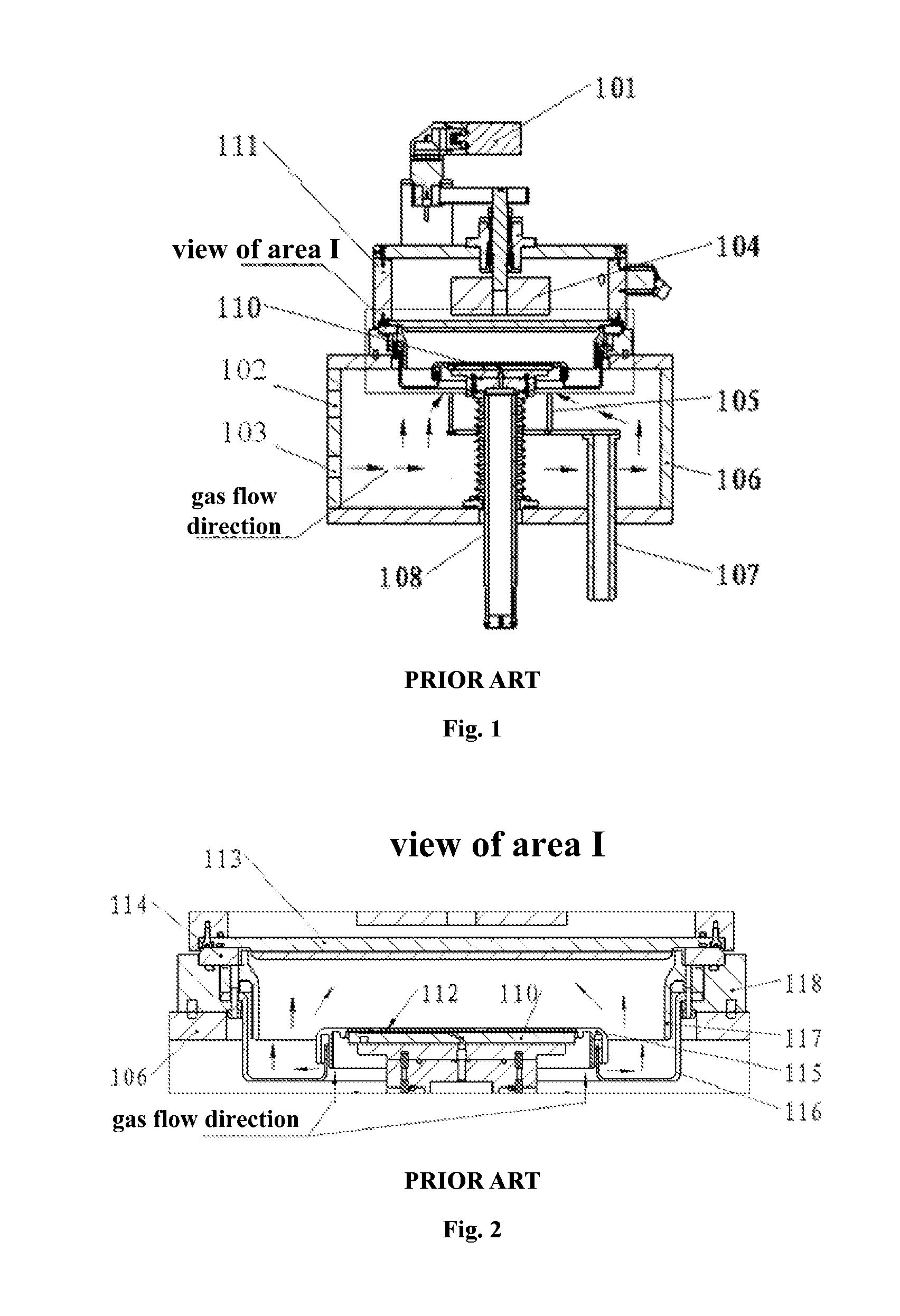
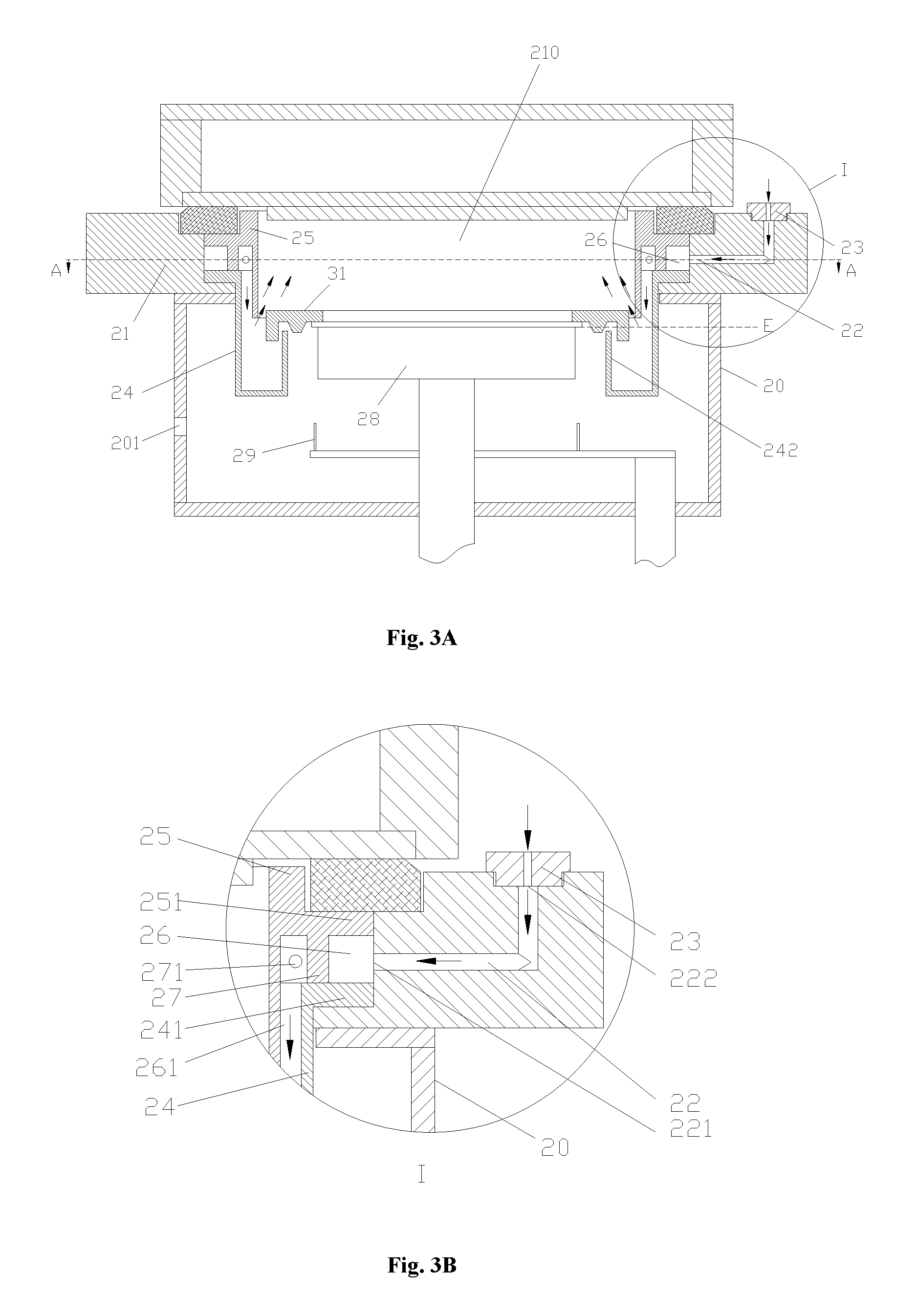
[0034]Advantages and features of the invention and methods of accomplishing the same will be apparent by referring to embodiments described below in detail in connection with the accompanying drawings. However, the invention is not limited to the embodiments disclosed below and may be implemented in various different forms. The embodiments are provided only for completing the disclosure of the invention and for fully representing the scope of the invention to those skilled in the art.

[0035]For simplicity and clarity of illustration, the drawing figures illustrate the general manner of construction, and descriptions and details of well-known features and techniques may be omitted to avoid unnecessarily obscuring the discussion of the described embodiments of the invention. Additionally, elements in the drawing figures are not necessarily drawn to scale. According to at least one embodiment, the dimensions of some of the elements in the figures may be exaggerated relative to other ele...


PUM

PropertyMeasurementUnit
Diameteraaaaaaaaaa
Diameteraaaaaaaaaa

Abstract

Embodiments of the invention provide a process chamber and a semiconductor processing apparatus. According to at least one embodiment, the process chamber includes a reaction compartment, a gas introducing system and a wafer transfer device. The reaction compartment is provided in the process chamber and used for performing a process on a wafer, the gas introducing system is used for providing processing gas to the reaction compartment, and the wafer transfer device is used for transferring the wafer into the reaction compartment. A lining ring assembly is provided in the reaction compartment, and is configured such that a flow uniformizing cavity is formed between the lining ring assembly itself and an inner side wall of the reaction compartment, so as to uniformly transport the processing gas, from the gas introducing system, into the reaction compartment through the flow uniformizing cavity.

Description

CROSS REFERENCE TO RELATED APPLICATION[0001]This application claims the benefit of and priority to PCT / CN2014 / 095338 filed on Dec. 29, 2014, entitled (translation), “PROCESS CHAMBER AND SEMICONDUCTOR PROCESSING APPARATUS,” which claims the benefit of and priority to Chinese Patent Application Nos. 201310737531.4 filed on Dec. 29, 2013, and 201410431336.3 filed on Aug. 28, 2014, both of which are entitled (translation), “PROCESS CHAMBER AND SEMICONDUCTOR PROCESSING APPARATUS,” and both of which are hereby incorporated by reference in their entirety into this application.BACKGROUND[0002]1. Field of the Invention[0003]Embodiments of the invention relate to the manufacturing field of a semiconductor apparatus, and more specifically relate to a process chamber and a semiconductor processing apparatus.[0004]2. Description of the Related Art[0005]A fundamental principle of physical vapor deposition (PVD) is that, under vacuum, a metal, or a metal alloy or a metal compound is evaporated and...

Claims


Application Information

Patent Timeline
IPC IPC(8): H01J37/32C23C14/00H01J37/34H01L21/67
CPCH01J37/32642H01L21/6719H01L21/67207H01J37/32853C23C14/0068H01J37/3411H01J37/32733H01L21/67167H01L21/67161H01L21/67739C23C14/34C23C14/564H01J37/34H01J37/32449H01J37/32633
Inventor LV, FENGZHANG, FENGGANGZHAO, MENGXINDING, PEIJUN
Owner BEIJING NAURA MICROELECTRONICS EQUIP CO LTD
Features
  • Generate Ideas
  • Intellectual Property
  • Life Sciences
  • Materials
  • Tech Scout
  • Unparalleled Data Quality
  • Higher Quality Content
  • 60% Fewer Hallucinations
Learn More