Silicon-photonics-based optical switch

a technology of optical switches and silicon photonics, applied in the field of optical switching, can solve the problems of increasing the difficulty of increasing the network bandwidth in this manner, the response time of such switches is limited to about 10 milliseconds, and the development of practical systems suitable for widespread deployment in such applications, etc., to achieve the effect of rapid and low-loss optical switching

Active Publication Date: 2016-11-10
RGT UNIV OF CALIFORNIA
View PDF4 Cites 40 Cited by
  • Summary
  • Abstract
  • Description
  • Claims
  • Application Information

AI Technical Summary

Benefits of technology

[0015]The present invention enables rapid, low-loss optical switching in a low-cost, practical switch technology. Embodiments of the present invention are well suited for use in telecom and datacom optical circuit switches, such as optical cross connects, wavelength-selective cross connects, reconfigurable optical add-drop multiplexers, 1×2 optical switches, and the like.

Problems solved by technology

In recent decades, however, practical and technological barriers have made it increasingly difficult to increase network bandwidth in this manner.
The development of practical systems suitable for widespread deployment in such applications—particularly, large-port-count OXCs, has proven challenging.
The response time of such switches, however, is limited to about 10 milliseconds while faster switching speeds are required in many applications.
Unfortunately, these switches comprise large numbers of cascaded 1×2 or 2×2 switches, each of which exhibits significant optical loss.
As a result, the cumulative optical loss along an optical path through the switch fabric is unacceptably high for many applications.
Unfortunately, such a switch fabric still includes 2*N*N waveguides and an optical signal path through such the switch fabric encompasses 2*log 2N switches.
As a result, the aggregate optical loss for an optical signal propagating through the switch fabric remains quite high.
Unfortunately, this approach has several drawbacks.
First, the freestanding waveguide portion must be quite long.
As a result, such an optical switch requires a great deal of chip real estate, which leads to high cost.
As a result, such optical switches are subject to path-dependent losses that vary considerably from path to path.
Path-dependent-loss variation can lead to complicated issues in systems employing such switches.
A practical, fast, low-cost, low-loss optical switching technology suitable for use in switching elements of low- and high-port counts remains, as yet, unavailable in the prior art.

Method used


Image

  • Silicon-photonics-based optical switch
  • Silicon-photonics-based optical switch
  • Silicon-photonics-based optical switch

Examples


Embodiment Construction

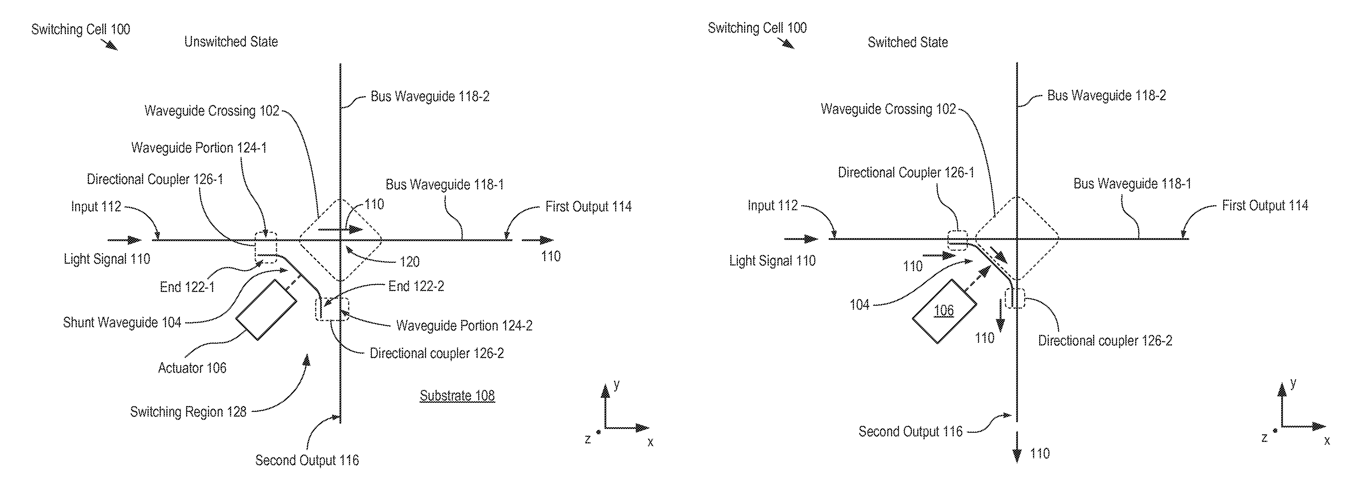
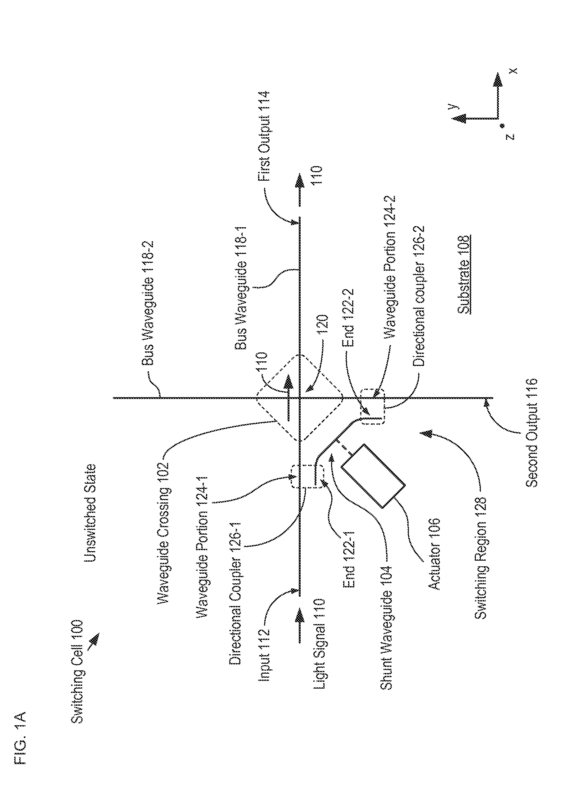
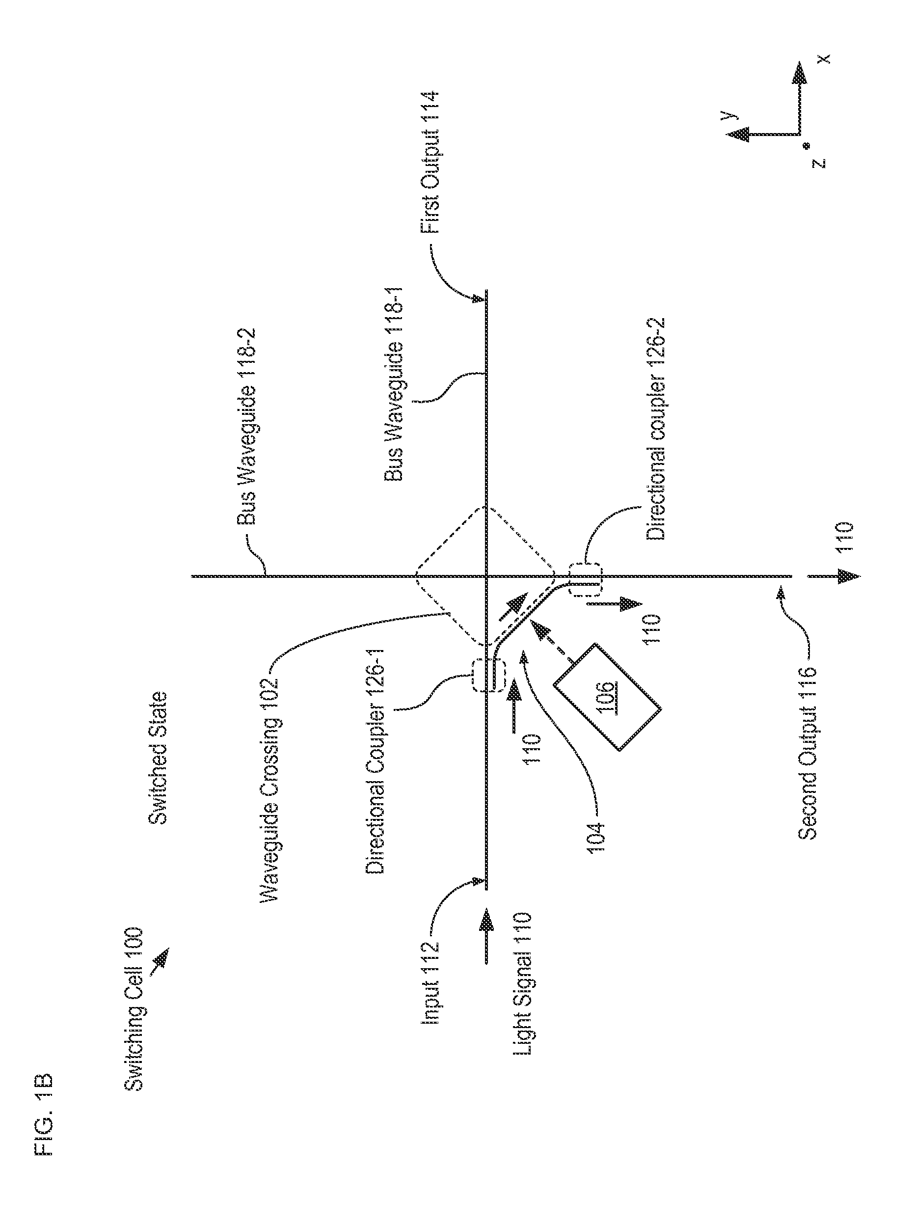
[0047]The most basic embodiment of the present invention is an optical switch comprising a 1×2 switching cell. By combining multiple switching cells in a monolithic planar lightwave circuit, more complex network element embodiments, such as M×N cross-connects, data network cross-point switches, wavelength add-drop multiplexers, and the like, can be developed and such embodiments are within the scope of the present invention. In order to readily afford an understanding of many of its fundamental principles, however, the description of the present invention begins with a simple 1×2 switching cell embodiment.

1×2 Switching Cell

[0048]FIGS. 1A and 1B depict schematic drawings of a 1×2 optical switching cell, in its unswitched and switched states, respectively, in accordance with an illustrative embodiment of the present invention. FIGS. 1A and 1B are simplified to facilitate demonstration of the operation of the switching cell. Switching cell 100 is a 1×2 optical circuit switch that inclu...


PUM


Abstract

An optical switching system comprising a switching cell having first and second fixed-position bus waveguides and a moveable shunt waveguide is disclosed. The first bus waveguide includes an input and a first output. The second bus waveguide includes a second output. When the switching cell is in its unswitched state, the shunt waveguide is not optically coupled with either bus waveguide and a light signal can pass from the input to the first output while remaining in the first bus waveguide. When the switching cell is in its switched state, the shunt waveguide is optically coupled with both bus waveguides such that the light signal is coupled out of the first bus waveguide and into the second bus waveguide via the shunt waveguide. As a result, the light signal can pass from the input to the second output while bypassing the first input.

Description

CROSS REFERENCE TO RELATED APPLICATIONS[0001]This case claims priority of U.S. Provisional Patent Application Ser. No. 61 / 926,276, filed Jan. 11, 2014 (Attorney Docket: BK-2014-115-1) and U.S. Provisional Patent Application Ser. No. 62 / 064,983, filed Oct. 16, 2014 (Attorney Docket: BK-2014-115-2), each of which is incorporated by reference.If there are any contradictions or inconsistencies in language between this application and one or more of the cases that have been incorporated by reference that might affect the interpretation of the claims in this case, the claims in this case should be interpreted to be consistent with the language in this case.STATEMENT REGARDING FEDERALLY SPONSORED RESEARCH[0002]This invention was made with Government support under Contract No. HR0011-11-2-0021 awarded by the Defense Advanced Projects Research Agency (DARPA) and Contract Number Y503161 awarded by the National Science Foundation (NSF). The Government has certain rights in the invention.FIELD ...

Claims


Application Information

Patent Timeline
Patent Type & Authority Applications(United States)
IPC IPC(8): G02B6/35G02B6/293
CPCG02B6/3504G02B6/355G02B6/3546G02B6/29344G02B6/3588G02B6/357G02B6/3596G02B6/3502G02B6/12007G02B6/136G02B6/356G02B6/3584G02B2006/12061G02B2006/12097G02B2006/12145G02B2006/12147G02B2006/12164
Inventor WU, MING C.HAN, SANGYOONSEOK, TAE JOONQUACK, NIELSYOO, BYUNG-WOOK
Owner RGT UNIV OF CALIFORNIA
Why Eureka
Try Eureka