Semiconductor chip with offloaded logic

a technology of semiconductor chips and logic, applied in semiconductor/solid-state device testing/measurement, automated testing systems, instruments, etc., can solve the problems of dft circuits rarely used by the end user, power and heat consumption, and large die area consumed by cutting edge process nodes

Pending Publication Date: 2016-11-10
ADVANCED MICRO DEVICES INC
View PDF16 Cites 32 Cited by
  • Summary
  • Abstract
  • Description
  • Claims
  • Application Information

AI Technical Summary

Problems solved by technology

While this can yield better performance, cutting edge process nodes can tend to have lower yields and higher costs.
As such, they consume die area, consume power and dissipate heat.
However, these DFT circuits are seldom used by the end user.
Since DFT circuit design must compete with other logic for die space, conventional DFT circuits often compromise performance to accommodate operational die logic.

Method used


Image

  • Semiconductor chip with offloaded logic
  • Semiconductor chip with offloaded logic
  • Semiconductor chip with offloaded logic

Examples


Embodiment Construction

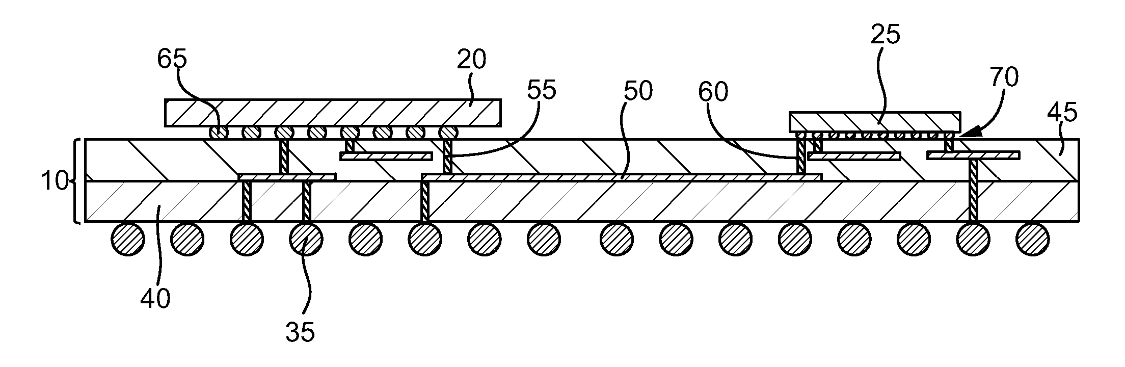
[0019]Various multi-semiconductor chip arrangements are disclosed. The disclosed embodiments take logic from one semiconductor chip and offload it to another semiconductor chip. The two chips are then electrically connected by an interposer. The first semiconductor chip can be wholly or partly fabricated at the most current process node, while the offloaded logic in the second semiconductor chip may be fabricated at an earlier process node where yields may be higher and costs lower. In this way, logic such as data path or DFT circuits can be offloaded and can function using the high speed pathways of the interposer. Additional details will now be disclosed.

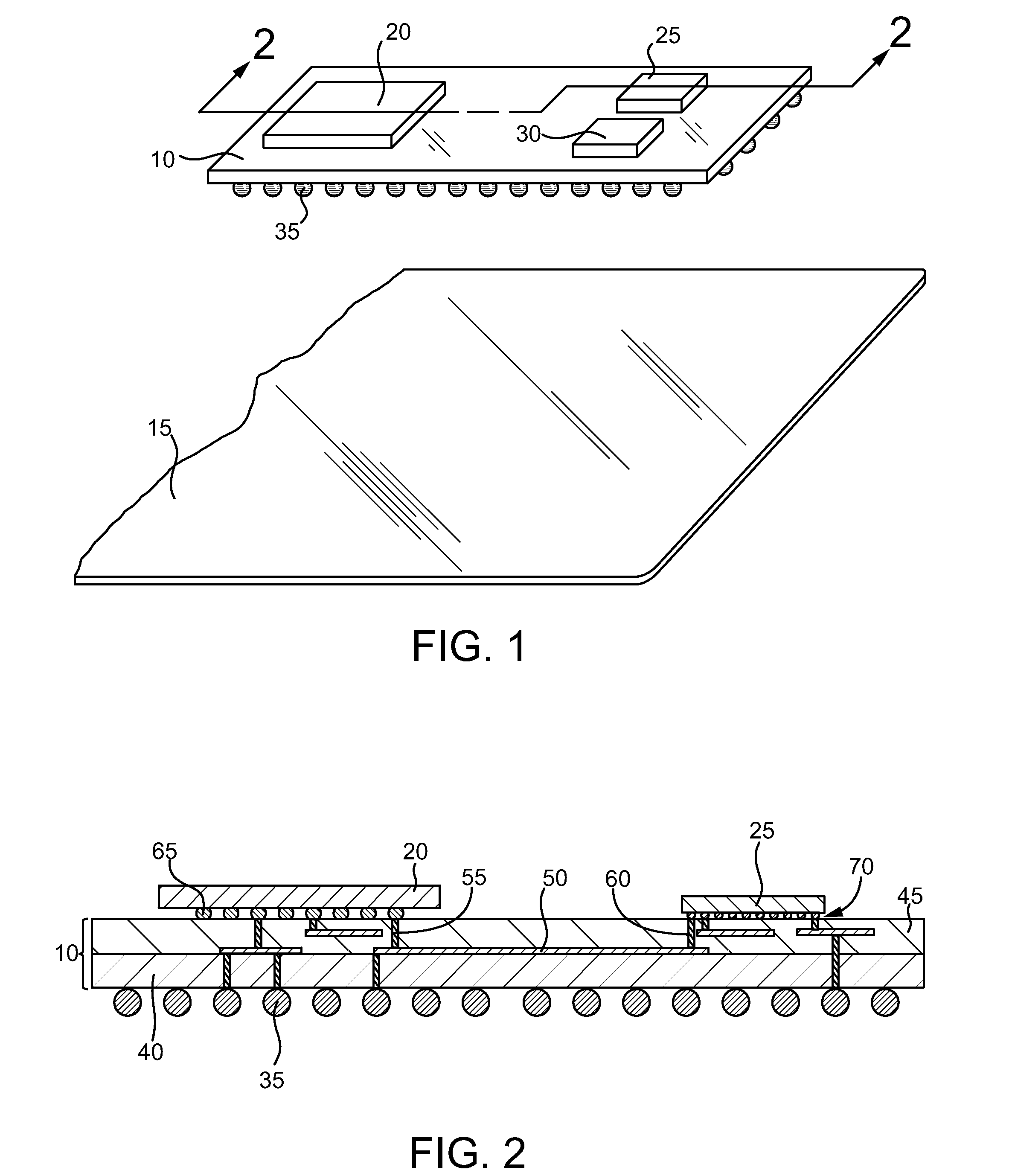
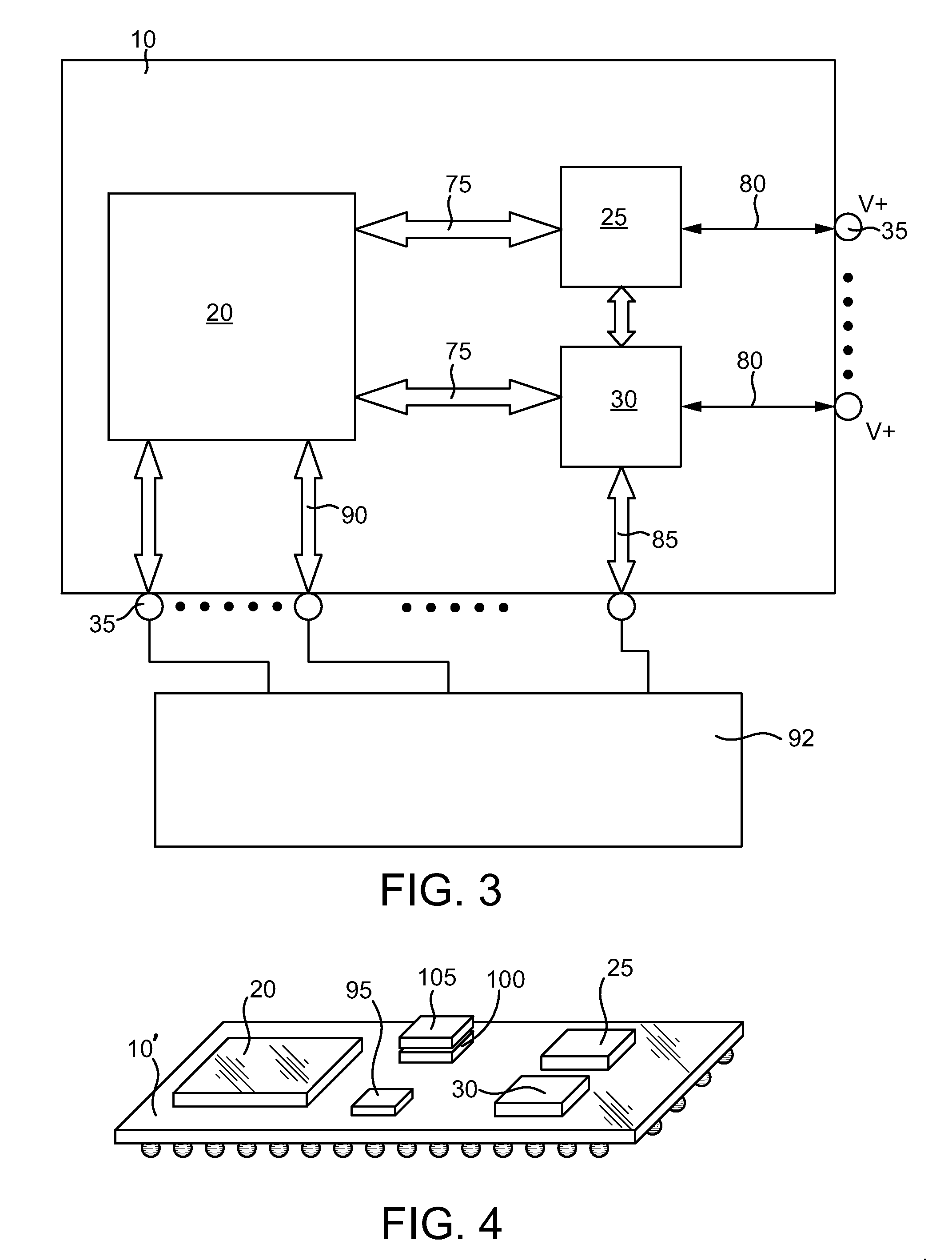
[0020]In the drawings described below, reference numerals are generally repeated where identical elements appear in more than one figure. Turning now to the drawings, and in particular to FIG. 1, therein is shown a pictorial view of an exemplary embodiment of an interposer 10 that is shown exploded from an exemplary circuit board ...


PUM


Abstract

Various semiconductor chip and interposer devices are disclosed. In one aspect, an apparatus is provided that includes an interposer, a first semiconductor chip mounted on the interposer and a second semiconductor chip mounted on and electrically connected to the first semiconductor chip by the interposer. The second semiconductor chip includes offloaded logic of the first semiconductor chip.

Description

BACKGROUND OF THE INVENTION[0001]1. Field of the Invention[0002]This invention relates generally to semiconductor processing, and more particularly to interposer based semiconductor chips and methods of using the same.[0003]2. Description of the Related Art[0004]Conventional microprocessor data paths typically consist of logic units to facilitate the movement and other processing of data. Conventional data paths are typically designed using a single process technology node. The newest generations of processors normally use the most current, and thus smallest geometry, process node to construct data path logic. While this can yield better performance, cutting edge process nodes can tend to have lower yields and higher costs.[0005]Design-for-Test (DFT) circuits are used to perform in-house testing various of aspects of conventional processors. Conventional DFT circuits are currently designed to be implemented directly into the microprocessor silicon. As such, they consume die area, co...

Claims


Application Information

Patent Timeline
Patent Type & Authority Applications(United States)
IPC IPC(8): H01L25/18G01R31/28H01L23/498H01L21/66H01L25/00
CPCH01L25/18H01L22/34G01R31/2834H01L23/49838G01R31/2884H01L25/50H01L23/49811H01L23/49822H01L23/49827H01L2224/131H01L2224/13144H01L2224/16227H01L2224/16235H01L2924/15192H01L2924/15311H01L2224/98H01L24/13H01L24/16H01L25/0652H01L25/0655H01L2224/16145H01L2924/10252H01L2924/10253H01L2924/14H01L2924/1432H01L2924/1433H01L2924/1434H01L2924/15312H01L2924/15313H05K1/181G01R31/2856H01L2924/014H01L2924/00014
Inventor O'MULLAN, SEAN M.ALFANO, MICHAEL S.BLACK, BRYAN
Owner ADVANCED MICRO DEVICES INC
Why Eureka
Try Eureka