

Planar magnetic element
a magnetic element and planar technology, applied in the field of planar magnetic elements, can solve the problems of difficult application of shielding emi noise methods, and achieve the effect of effectively reducing emi nois
- Summary
- Abstract
- Description
- Claims
- Application Information
AI Technical Summary
Benefits of technology
Problems solved by technology
Method used
Image

Examples
first embodiment
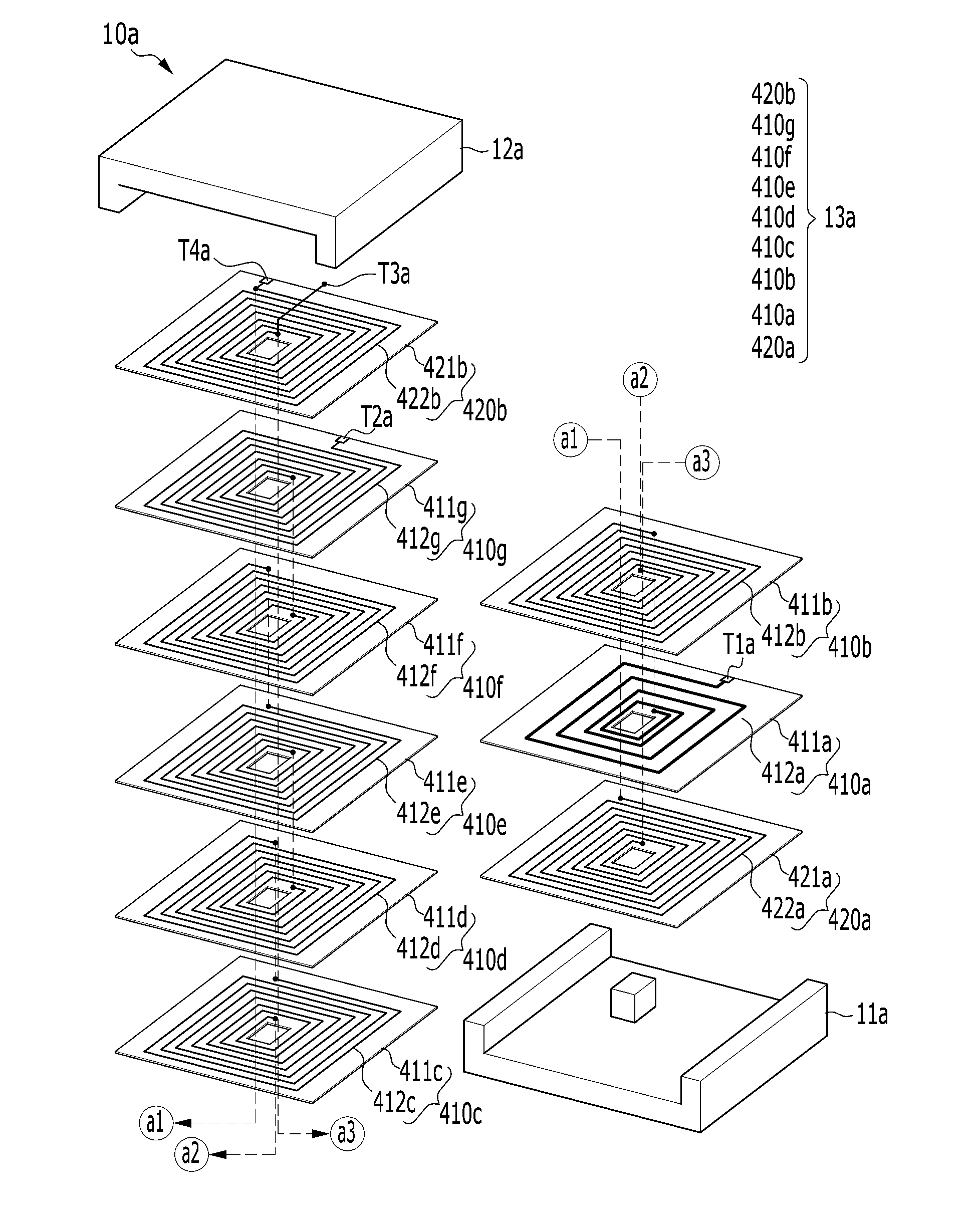
[0074]FIG. 4 is a view illustrating a planar magnetic element according to a
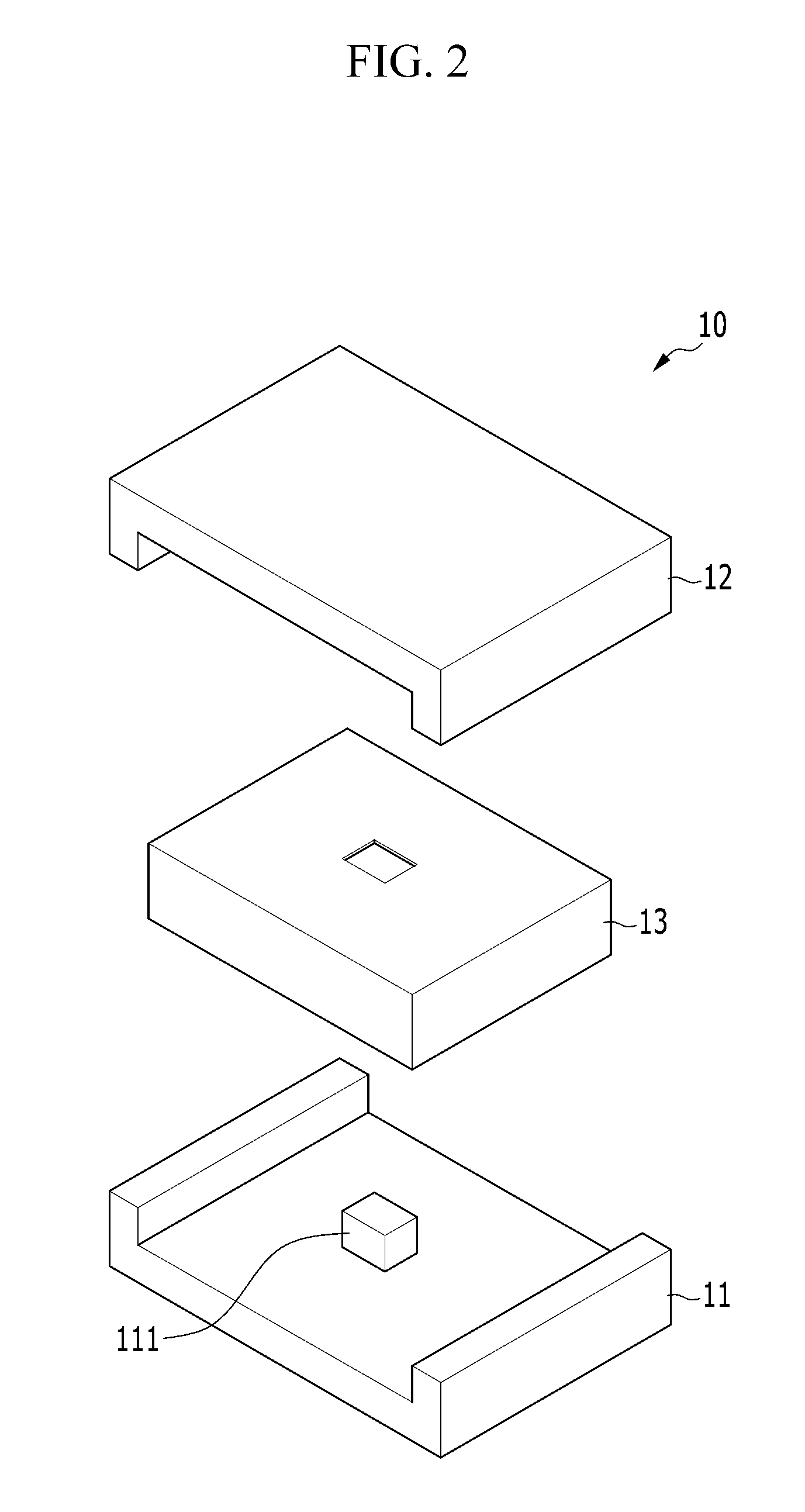
[0075]Referring to FIG. 4, a planar magnetic element 10a according to a first embodiment includes a pair of cores 11a and 12a and a winding unit 13a disposed between the pair of cores 11a and 12a.
[0076]The winding unit 13a includes winding layers 410a to 410g stacked between the pair of cores 11a and 12a.
[0077]The main winding layers 410a to 410g include substrates 411a to 411g and windings 412a to 412g disposed on the substrates 411a to 411g, respectively. The substrates 411a to 411g of the main winding layers 410a to 410g are formed with an insulating material and include through-holes H into which legs of the cores 11a and 12a are inserted. The windings 412a to 412g of the main winding layers 410a to 410g are formed with metallic materials with high conductivity and are formed with conductive patterns having inductance. For example, the windings 412a to 412g of the main winding layers 410a to 410g may b...
second embodiment
[0086]FIG. 5 is a view illustrating a planar magnetic element 10b and illustrates a case in which windings 522a and 522b of auxiliary winding layers 520a and 520b are connected to each other in series.
[0087]Referring to FIG. 5, one end of the winding 522a is connected to a fourth terminal T4b, one end of the winding 522b is connected to a third terminal T3b, and the other end 522a-1 of the winding 522a and the other end 522b-1 of the winding 522b are connected to each other. When the windings 522a and 522b of the auxiliary winding layers 520a and 520b are connected to each other in series as illustrated in FIG. 5, the thicknesses, the cross-sectional areas, the winding numbers, etc. of the windings may be formed differently compared to the case in which the windings 422a and 422b of the auxiliary winding layers 420a and 420b are connected to each other in parallel as illustrated in FIG. 4. When the windings 522a and 522b of the auxiliary winding layers 520a and 520b are connected t...
third embodiment
[0090]FIG. 6 is a view illustrating a planar magnetic element according to a
[0091]Referring to FIG. 6, a planar magnetic element 10c according to a third embodiment includes a pair of cores 11c and 12c and a winding unit 13c disposed between the pair of cores 11c and 12c.
[0092]The winding unit 13c includes a plurality of main winding layers 610a to 610g stacked between the pair of cores 11c and 12c.
[0093]The main winding layers 610a to 610g include substrates 611a to 611g and windings 612a to 612g and 613b to 613g disposed on the substrates 611a to 611g, respectively.
[0094]The windings 612a to 612g and 613b to 613g included in the plurality of main winding layers 610a to 610g are connected between a first terminal T1c and a second terminal T2c to form a main winding of the planar magnetic element 10c.
[0095]Some of the main winding layers 610b to 610g among the plurality of main winding layers 610a to 610g include windings 612b to 612g (hereinafter referred to as “inner windings”)...
PUM
| Property | Measurement | Unit |
|---|---|---|
| planar magnetic | aaaaa | aaaaa |
| winding widths | aaaaa | aaaaa |
| size | aaaaa | aaaaa |
Abstract
Description
Claims
Application Information