IMS formed as can for semiconductor housing

a technology of semiconductor housing and cannon, which is applied in the direction of semiconductor/solid-state device details, semiconductor devices, electrical apparatus, etc., can solve the problems of poor thermal performance and high inductance of direct fet packages, and achieve the effect of reducing the emi noise generated by the packages and high placement accuracy and process control

Active Publication Date: 2012-01-03
INFINEON TECH AMERICAS CORP
View PDF6 Cites 7 Cited by
  • Summary
  • Abstract
  • Description
  • Claims
  • Application Information

AI Technical Summary

Benefits of technology

[0015]The benefit of this arrangement of electrodes is that it permits mounting of smaller die in the package than a customer could otherwise handle in their conventional pick-and-place and soldering operations. This is a consequence of being able to achieve higher placement accuracy and process control in forming the solder joints.
[0016]Second, removing the substrate as the switch node in the half bridge will reduce EMI noise generated by the package and also isolates any heat sink placed on the package from any live terminal.
[0021]Compared to wire bonded packages; a reduced inductance; reduced RDSON; improved thermal performance;

Problems solved by technology

These, however, will have a higher inductance and higher RDSON than a copack in a Direct FET package and have poorer thermal performance than that of the Direct FET packages.

Method used


Image

  • IMS formed as can for semiconductor housing
  • IMS formed as can for semiconductor housing
  • IMS formed as can for semiconductor housing

Examples


Embodiment Construction

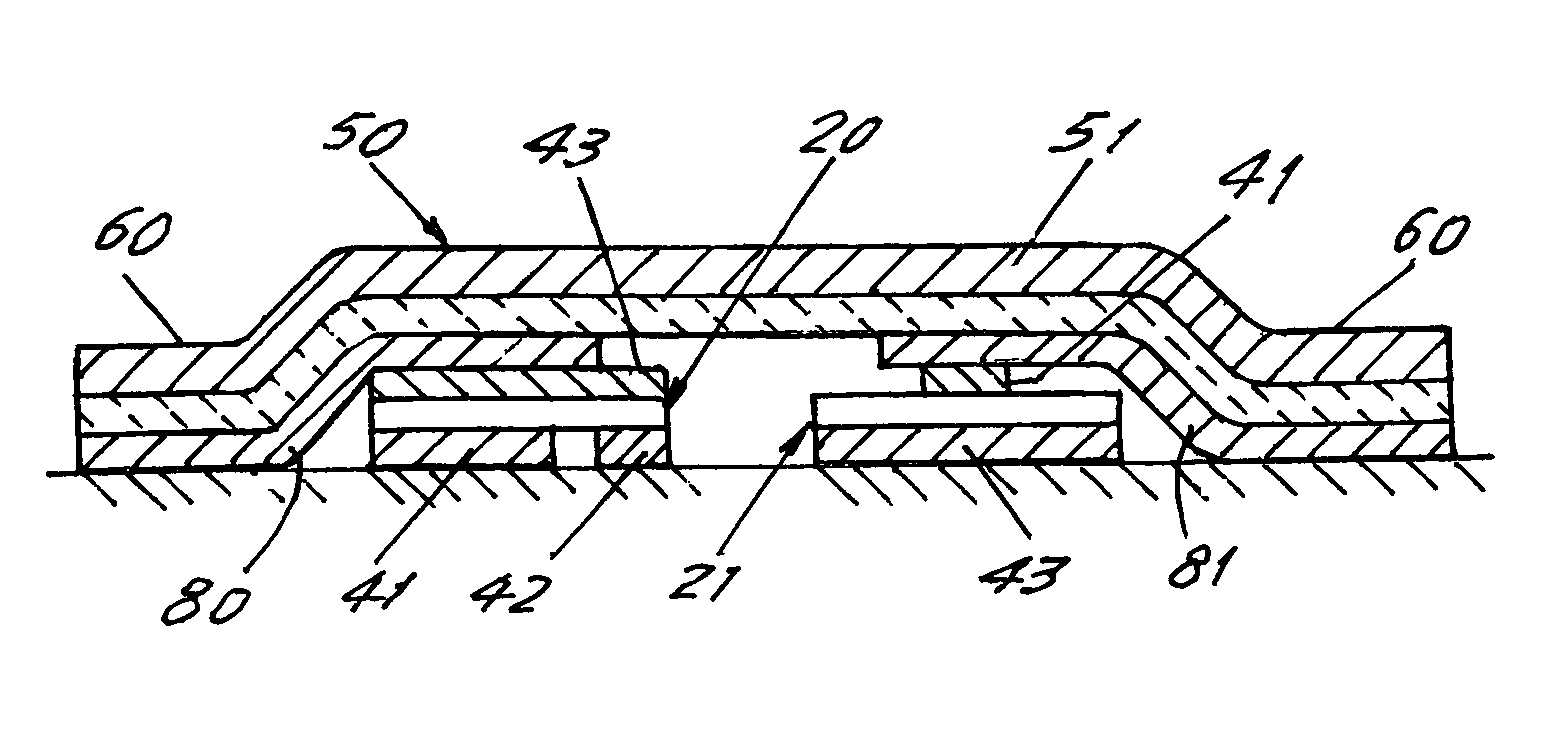
[0037]Referring first to FIG. 1, the circuit shown is a buck converter circuit comprising a control MOSFET 20, a synchronous MOSFET 21 and a control IC 23 which controls FETs 20 and 21 as usual. An input d-c voltage is applied to terminal V(+) and to the half bridge circuit formed by FETs 20 and 21. The source S of FET 21 is connected to terminal V(−) (or ground) and the node of the source terminal of FET 20 and the drain terminal of FET 21 is connected to output terminal “out”. The output terminal then has an appropriate voltage connected to load 30 through inductor 31 and output capacitor 32.

[0038]In accordance with the invention, FETs 20 and 21 are copacked in the common housing 22, which is a Direct FET style housing as will be described.

[0039]Each of MOSFETs 20 and 21 can have any desired structure and topology and can be planar or trench type devices. More specifically. They can be any type of MOSgated device including IGBTs. Further, the die may be silicon-based or III Nitrid...


PUM


Abstract

An insulated metal substrate composite has a patterned conductive layer on one surface and receives one or more electrodes of MOSFETs or other die on the patterned segments which lead to the edge of the IMS. The outer periphery of the IMS is cupped or bent to form a shallow can with two or more die fixed to and thermally coupled to the flat web of the can while electrodes on the die surfaces thermally coupled to the web of the can lead to terminals on the rim of the can which are coplanar with the bottom surfaces of the die. The electrodes can be externally or internally connected to form a half bridge circuit.

Description

RELATED APPLICATIONS[0001]This application claims the benefit of U.S. Provisional Application No. 60 / 732,625, filed Nov. 2, 2005, the entire disclosure of which is incorporated by reference herein.FIELD OF THE INVENTION[0002]This invention relates to semiconductor devices and more specifically relates to a novel package for semiconductor devices.BACKGROUND OF THE INVENTION[0003]U.S. Pat. No. 6,624,522 (IR-1830) shows a semiconductor package known by the trademark Direct FET, a trademark of the International Rectifier Corporation, in which semiconductor die are contained within a conductive clip or flat cup with one surface of the die connected to the interior surface of the clip and with the opposite surface and its electrodes generally coplanar with the bottom of the clip so that it can be conductively fastened to a support circuit board. The clip itself may be a contact for electrodes of the die connected to the interior of the clip, with all device electrodes being available for ...

Claims


Application Information

Patent Timeline
Patent Type & Authority Patents(United States)
IPC IPC(8): H01L23/34
CPCH01L25/072H01L25/162H01L2224/73153H01L2924/01077H01L2924/01079H01L2924/13091H01L2924/13055H01L2924/00
Inventor PAVIER, MARKBUSHNELL, DAVID
Owner INFINEON TECH AMERICAS CORP
Why Eureka
Try Eureka