Method of forming semiconductor structure

a technology of semiconductor structure and fin structure, which is applied in the direction of semiconductor devices, basic electric elements, electrical appliances, etc., can solve the problems of narrow width of each fin structure, shrinkage of the spacing between the fin structures, and the inability to achieve the required demands of forming fin structures. , to achieve the effect of precise layout of the fin structur

Inactive Publication Date: 2016-11-17
UNITED MICROELECTRONICS CORP
View PDF6 Cites 21 Cited by
  • Summary
  • Abstract
  • Description
  • Claims
  • Application Information

AI Technical Summary

Benefits of technology

[0008]According to the above, the method of forming fin shaped structures of present invention is accomplished by forming liners in rectangular shape, removing a portion of the liners and the mandrels due to the etching selectivity therebetween, and using the rest of liners as a mask to form the fin shaped structures. By using the aforementioned approach it may be desirable to form fin shaped structures with a finer size or a finer pitch, for forming more precise layout of the fin shaped structures

Problems solved by technology

However, as the size of the field effect transistors (FETs) is continuously shrunk, the development of the planar FETs faces more limitations in the fabricating process thereof, so that, non-planar FETs, such as the fin field effect transistor (finFET) having a three-dimensional structure have replaced the planar FETs and become the mainstream of the development.
However, with the demands of miniaturization of semiconductor devices, the width of each fin-shaped structure narrows and the spacing between the fin shaped structures shrinks.
Thus, forming fin shaped structures which can achieve the required demands under the restrictions of miniaturization, physical limitations and various processing parameters becomes an extreme challenge.

Method used


Image

  • Method of forming semiconductor structure
  • Method of forming semiconductor structure
  • Method of forming semiconductor structure

Examples


first embodiment

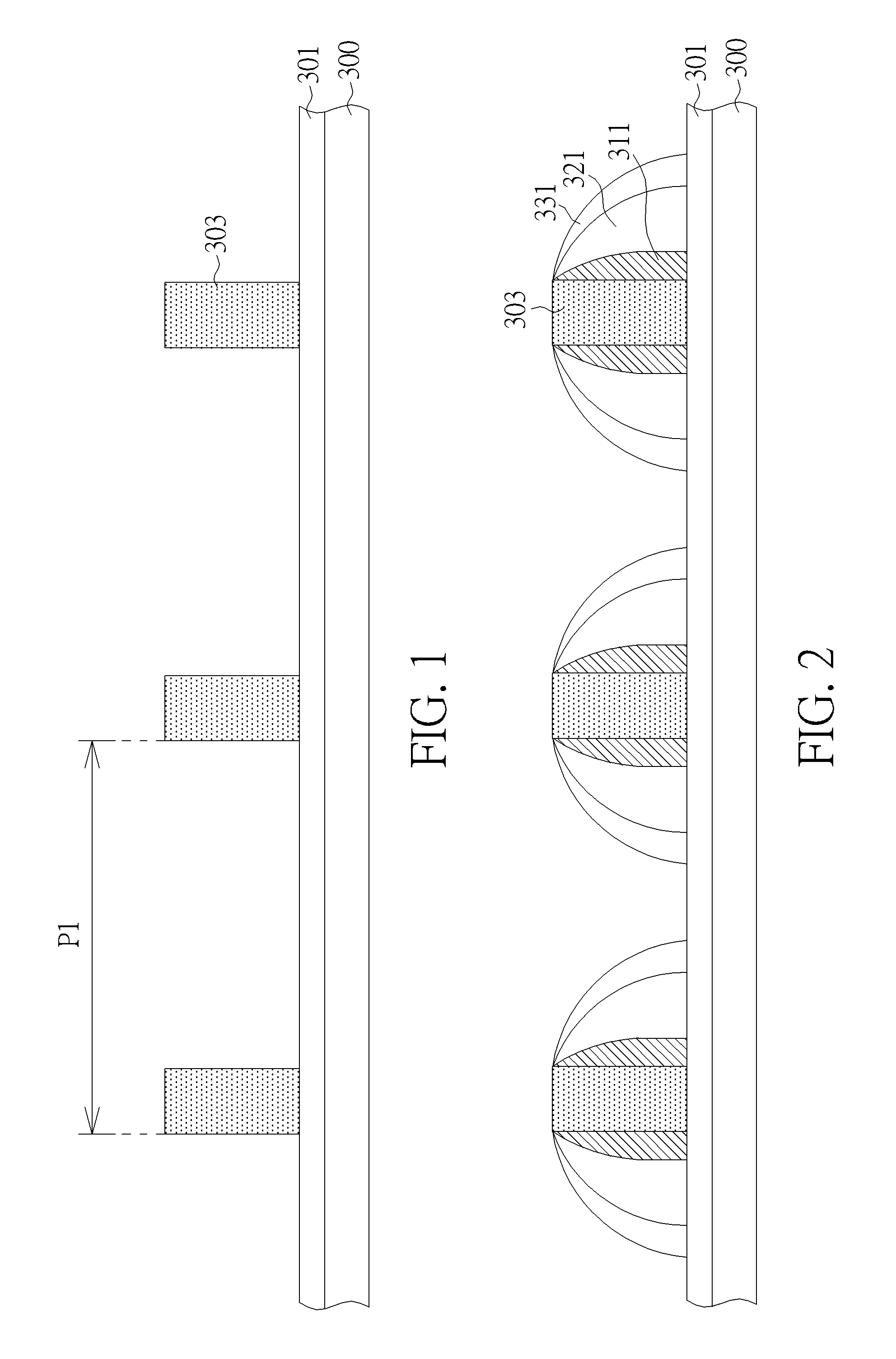
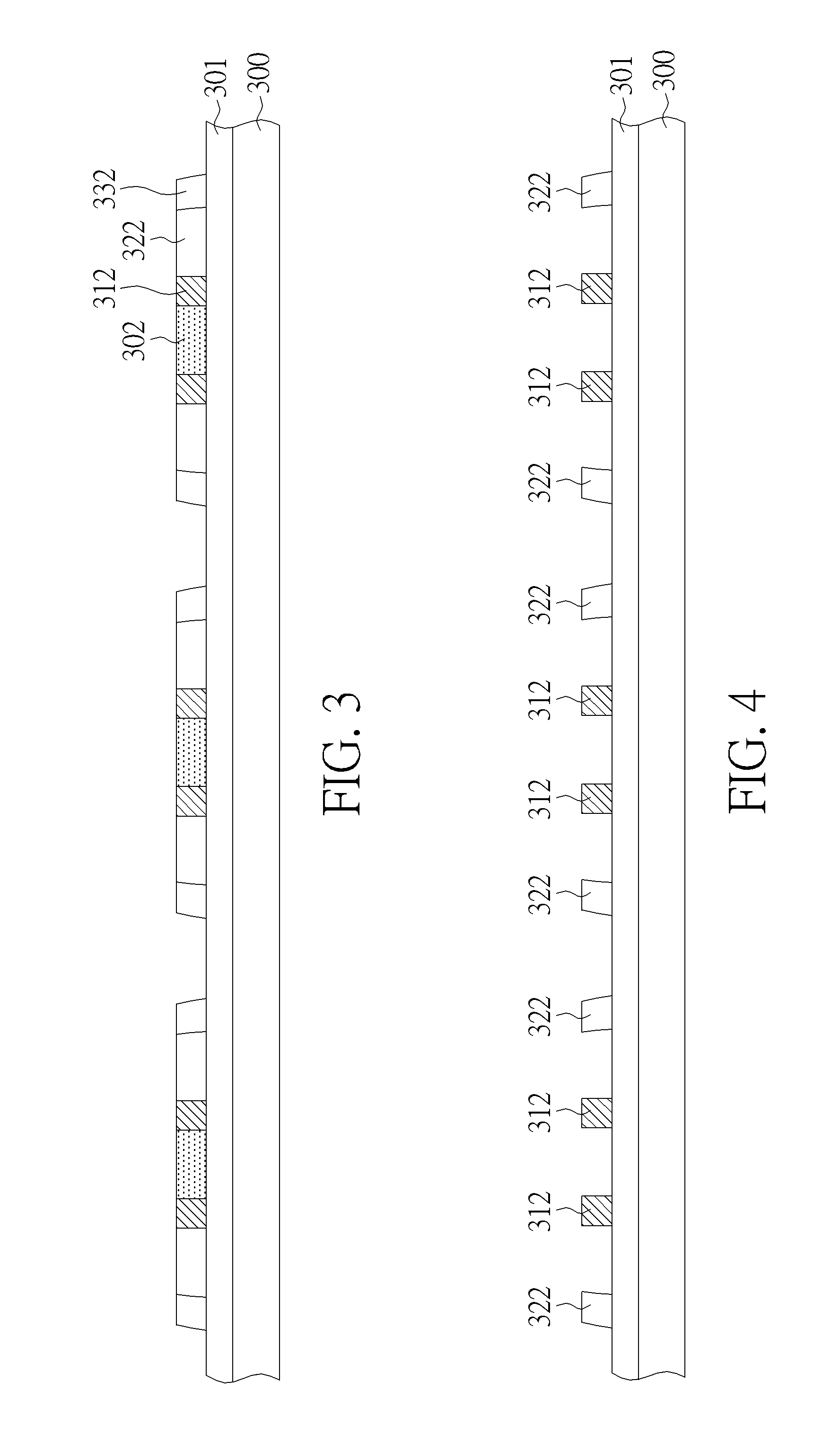
[0015]Please refer to FIG. 1 to FIG. 4, which are schematic diagrams illustrating a method of forming a semiconductor structure according to the present invention. First of all, a target layer is provided, which may include a semiconductor layer 300 shown in FIG. 1, such as a silicon layer, an epitaxial silicon layer, a silicon carbide layer or silicon on insulation (SOI) layer, but is not limited thereto. In another embodiment, the target layer may include a conductive layer, such as an aluminum (Al) layer, a copper (Cu) layer or a tungsten (W) layer; or a non-conductive layer, such as a dielectric layer, but is not limited thereto.

[0016]Next, as shown in FIG. 1, a plurality of mandrels 303 is formed on the semiconductor layer 300 (namely, the target layer). In the present embodiment, the formation of the mandrels 303 may be integrated with the general semiconductor fabrication process. For example, a gate process may be performed to form a plurality of gate patterns which serve as...

second embodiment

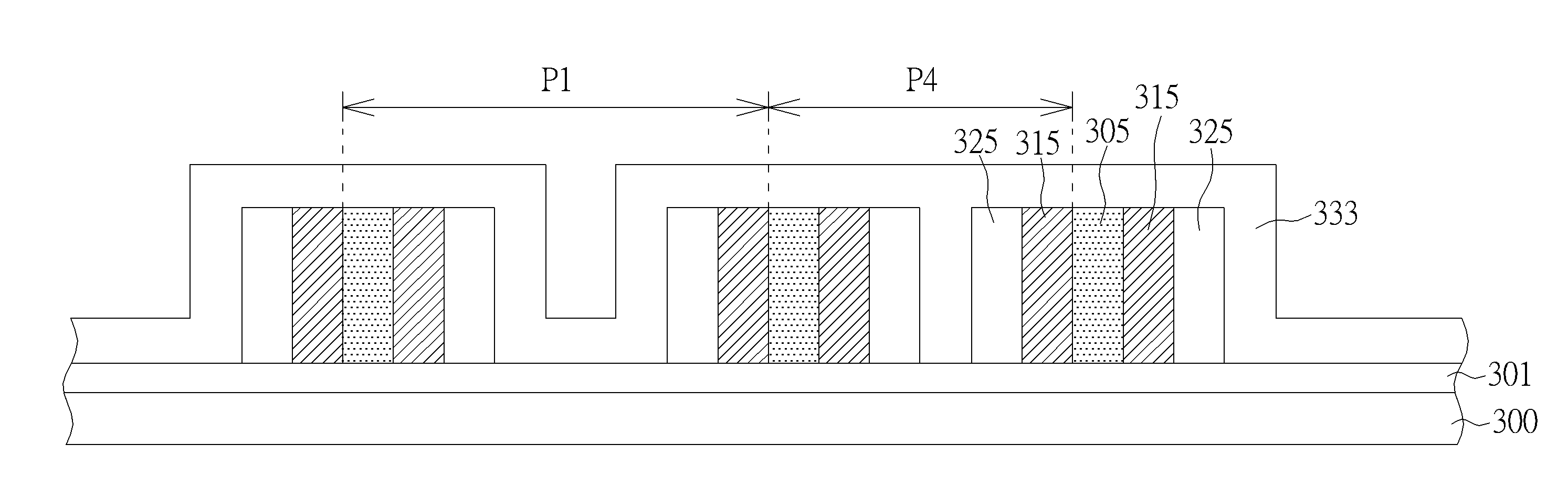
[0030]Through the above mentioned steps, the semiconductor structure according to the present invention is obtained. In the present embodiment, plural rectangular liners are formed directly, a portion of the rectangular liners is selectively removed due to the etching selectivity therebetween, and the rest of the rectangular liners may be used as a mask in the subsequent process to form fin shaped structures. With such performance, the etching mask with regular patterns may be sufficiently provided, so as to easily and conveniently form a desired layout of uniform fin shaped structures having the same widths, for forming more precise layout of the fin shaped structures.

[0031]Please refer to FIG. 9 to FIG. 10, which is a schematic diagram illustrating a method of forming a semiconductor structure according to the third embodiment of the present invention. The formal steps in the present embodiment are similar to those in the second embodiment, and the differences between the present ...


PUM


Abstract

A method of forming a semiconductor structure includes following steps. First of all, a plurality of mandrels is formed on a target layer. Next, a plurality of first liner is formed adjacent to two sides of the mandrels. Then, a plurality of second liners is formed adjacent to two sides of the first liners. After these, a plurality of third liners is formed adjacent to two sides of the second liners. Finally, the mandrels and the second liners are simultaneously removed.

Description

BACKGROUND OF THE INVENTION[0001]1. Field of the Invention[0002]The invention relates to a method of forming a semiconductor structure, and more particularly, to a method using spacer self-aligned quartic-patterning (SAQP) technique transferring patterns to form fin shaped structures.[0003]2. Description of the Prior Art[0004]With increasing miniaturization of semiconductor devices, it is crucial to maintain the efficiency of miniaturized semiconductor devices in the industry. However, as the size of the field effect transistors (FETs) is continuously shrunk, the development of the planar FETs faces more limitations in the fabricating process thereof, so that, non-planar FETs, such as the fin field effect transistor (finFET) having a three-dimensional structure have replaced the planar FETs and become the mainstream of the development. Since the three-dimensional structure of a finFET increases the overlapping area between the gate and the fin shaped structure of the silicon substra...

Claims


Application Information

Patent Timeline
Patent Type & Authority Applications(United States)
IPC IPC(8): H01L21/308H01L29/66H01L21/8234H01L21/311
CPCH01L21/3086H01L21/31144H01L21/3088H01L21/823431H01L29/6656H01L29/66795H01L21/0337H01L21/32139
Inventor LIOU, EN-CHIUANTUNG, YU-CHENG
Owner UNITED MICROELECTRONICS CORP
Why Eureka
Try Eureka