Method for electrical switching in oxide semiconductor device

Inactive Publication Date: 2016-11-17
PUKYONG NAT UNIV IND ACADEMIC COOPERATION FOUND
View PDF3 Cites 0 Cited by
  • Summary
  • Abstract
  • Description
  • Claims
  • Application Information

AI Technical Summary

Benefits of technology

[0009]An object of the present invention is to provide an electrical switching method for an oxide semiconductor device, whic

Problems solved by technology

As a result, the electrical gating-based power switching semiconductor is likely to malfunction.
Since battery capacity cannot be increase

Method used


Image

  • Method for electrical switching in oxide semiconductor device
  • Method for electrical switching in oxide semiconductor device
  • Method for electrical switching in oxide semiconductor device

Examples


Example

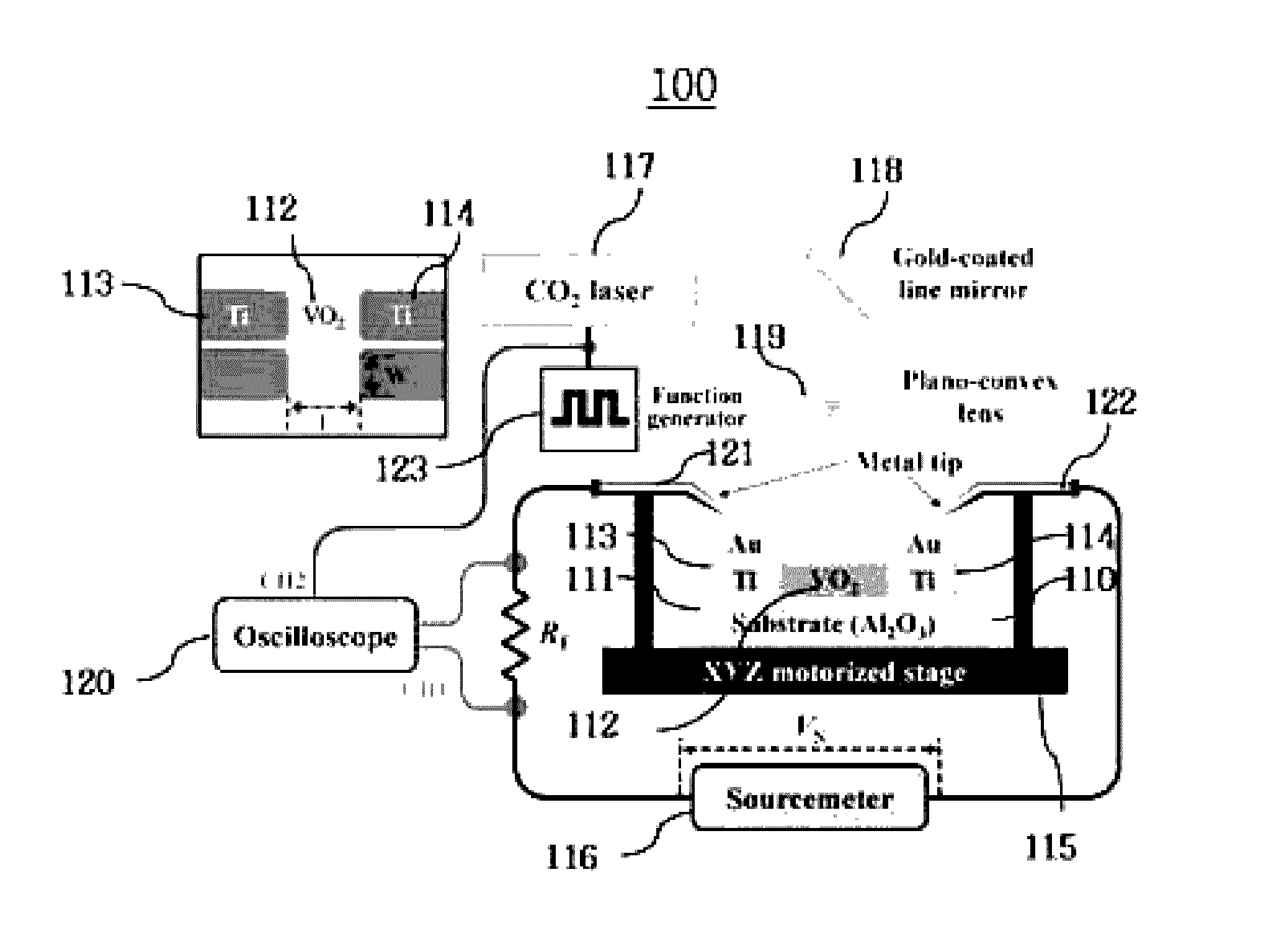
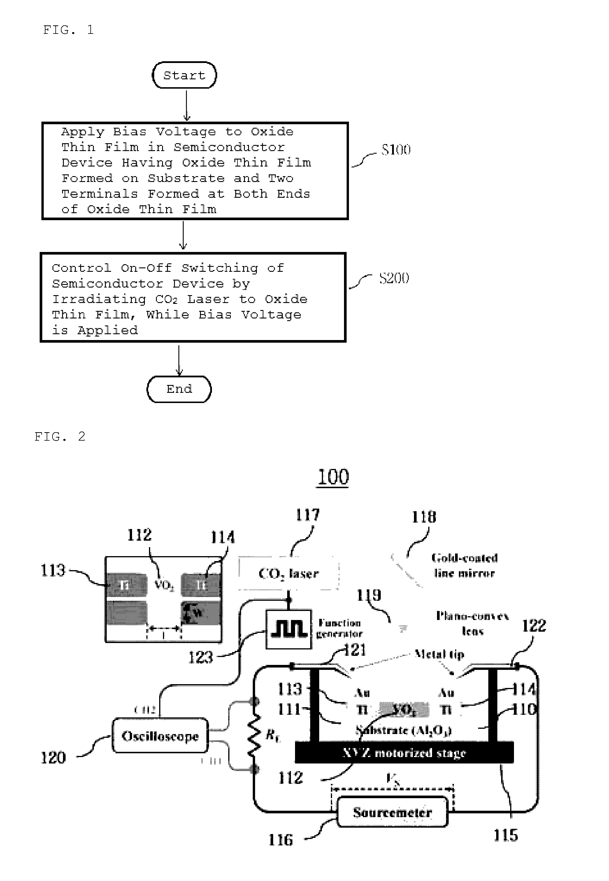
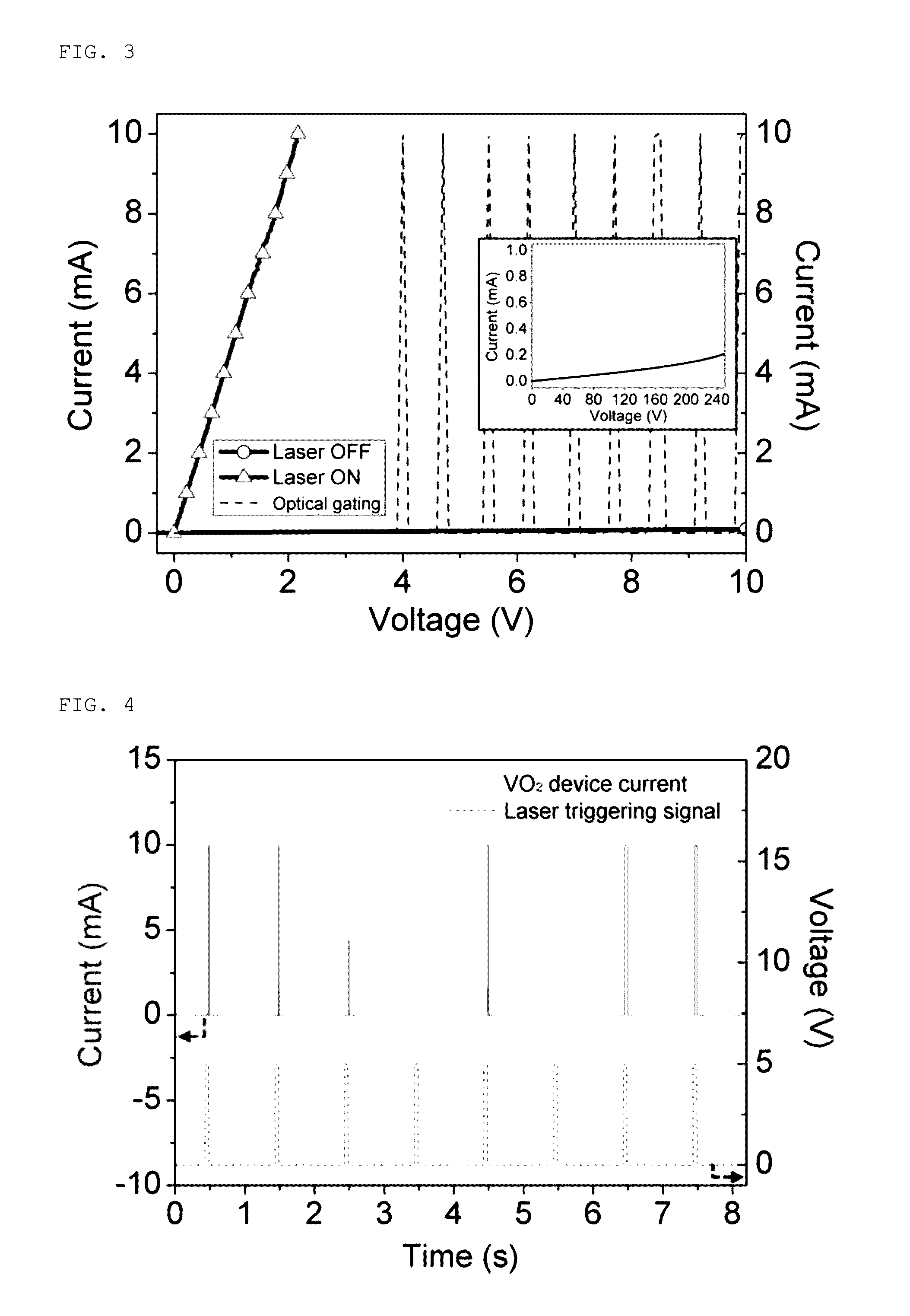
[0028]The objects and effects of the present invention and technical structures to achieve them will become apparent to those having ordinary skill in the art upon examination of the following embodiments of the present invention described with reference to the attached drawings. A detailed description of known functions or constructions will be omitted lest it should obscure the subject matter of the present invention. Terms used herein are defined in consideration of structures, roles, and functions according to the present invention and may be changed according to the intention of a user or an operator or customs.

[0029]However, the present invention is not limited to the embodiments described below. Rather, the present invention may be implemented in many other ways. The embodiments of the present invention are provided to make the disclosure of the present invention comprehensive and give a comprehensive scope of the present invention to those skilled in the art. The present inv...


PUM


Abstract

A method for electrical switching in an oxide semiconductor device is disclosed. The method includes applying a bias voltage to an oxide thin film of the semiconductor device, the semiconductor device having the oxide thin film formed on a substrate and two terminals formed at both ends of the oxide thin film, and controlling on-off switching of the semiconductor device by irradiating a carbon dioxide (CO2) laser to the oxide thin film, while the bias voltage is applied.

Description

[0001]This application claims the benefit of Korean Patent Application No. 10-2015-0068155, filed on May 15, 2015, which is hereby incorporated by reference as if fully set forth herein.BACKGROUND OF THE INVENTION[0002]1. Field of the Invention[0003]The present invention generally relates to a method for electrical switching in an oxide semiconductor device, and more particularly, to a method for performing electrical switching in an oxide semiconductor device by irradiating a carbon dioxide (CO2) laser beam to a vanadium dioxide (VO2) thin film.[0004]2. Discussion of the Related Art[0005]An electrical gating-based power switching semiconductor, which is a core device used for a high-power inverter attracting attention recently, such as a high voltage DC transmission system and a flexible AC transmission system, needs a plurality of additional circuits and an auxiliary power source, for monitoring and triggering. As a result, the electrical gating-based power switching semiconductor...

Claims


Application Information

Patent Timeline
IPC IPC(8): H03K17/78
CPCH03K17/78
Inventor LEE, YONGWOOKKIM, JIHOON
Owner PUKYONG NAT UNIV IND ACADEMIC COOPERATION FOUND
Why Eureka
Try Eureka