Light irradiation type heat treatment apparatus
- Summary
- Abstract
- Description
- Claims
- Application Information
AI Technical Summary
Benefits of technology
Problems solved by technology
Method used
Image

Examples
Embodiment Construction
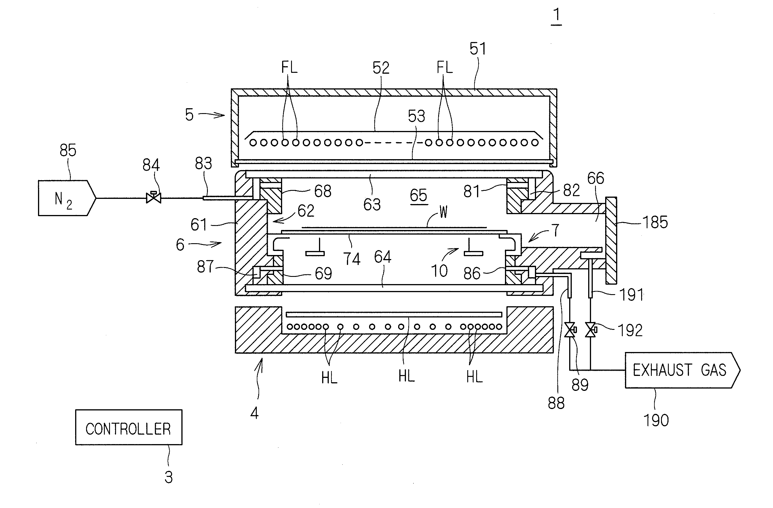
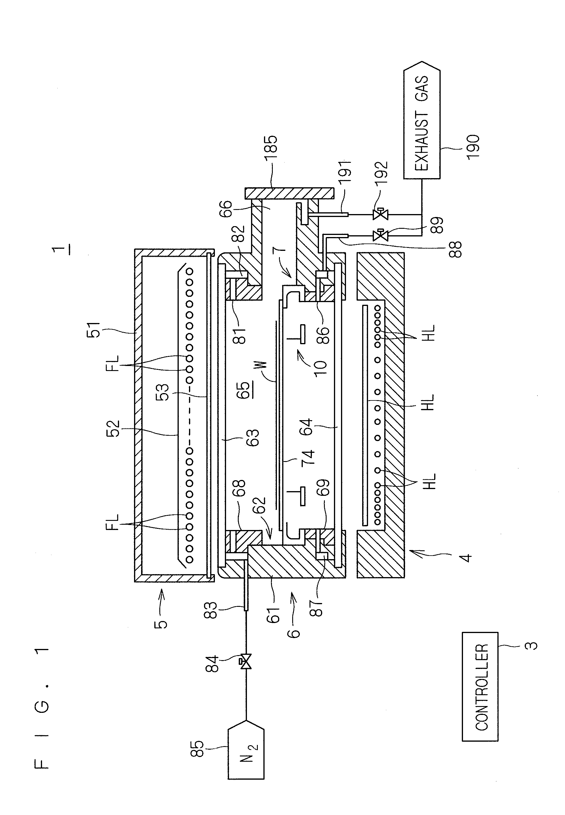
[0026]The following describes an embodiment of the present invention with reference to the drawings.
[0027]FIG. 1 is a longitudinal cross-sectional view showing a configuration of a heat treatment apparatus 1 according to the present invention. The heat treatment apparatus 1 in this embodiment is a flash-lamp annealing apparatus that heats a semiconductor wafer W having a disc shape and serving as a substrate by irradiating the semiconductor wafer W with flash light. While the size of the semiconductor wafer W to be treated is not particularly limited, the semiconductor wafer W has a diameter of 300 mm or 450 mm, for example. The semiconductor wafer W before being transported into the heat treatment apparatus 1 is implanted with impurities, and the heat treatment apparatus 1 performs heating treatment to activate the implanted impurities. To facilitate the understanding, the size and number of each part are exaggerated or simplified as necessary in FIG. 1 and subsequent drawings.
[002...
PUM
 Abstract
Description
Claims
Application Information
 - R&D Engineer
- R&D Manager
- IP Professional
- Industry Leading Data Capabilities
- Powerful AI technology
- Patent DNA Extraction
Browse by: Latest US Patents, China's latest patents, Technical Efficacy Thesaurus, Application Domain, Technology Topic.
© 2024 PatSnap. All rights reserved.Legal|Privacy policy|Modern Slavery Act Transparency Statement|Sitemap