Edge Coupler
a technology of edge couplers and couplers, applied in the field of optical couplers, can solve the problems of limited bandwidth, high observation loss, and limited optical mod
- Summary
- Abstract
- Description
- Claims
- Application Information
AI Technical Summary
Benefits of technology
Problems solved by technology
Method used
Image
Examples
first example embodiment
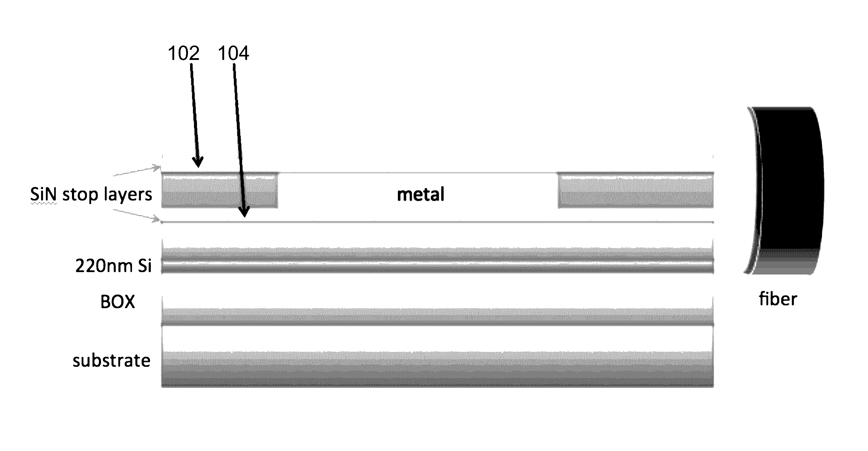
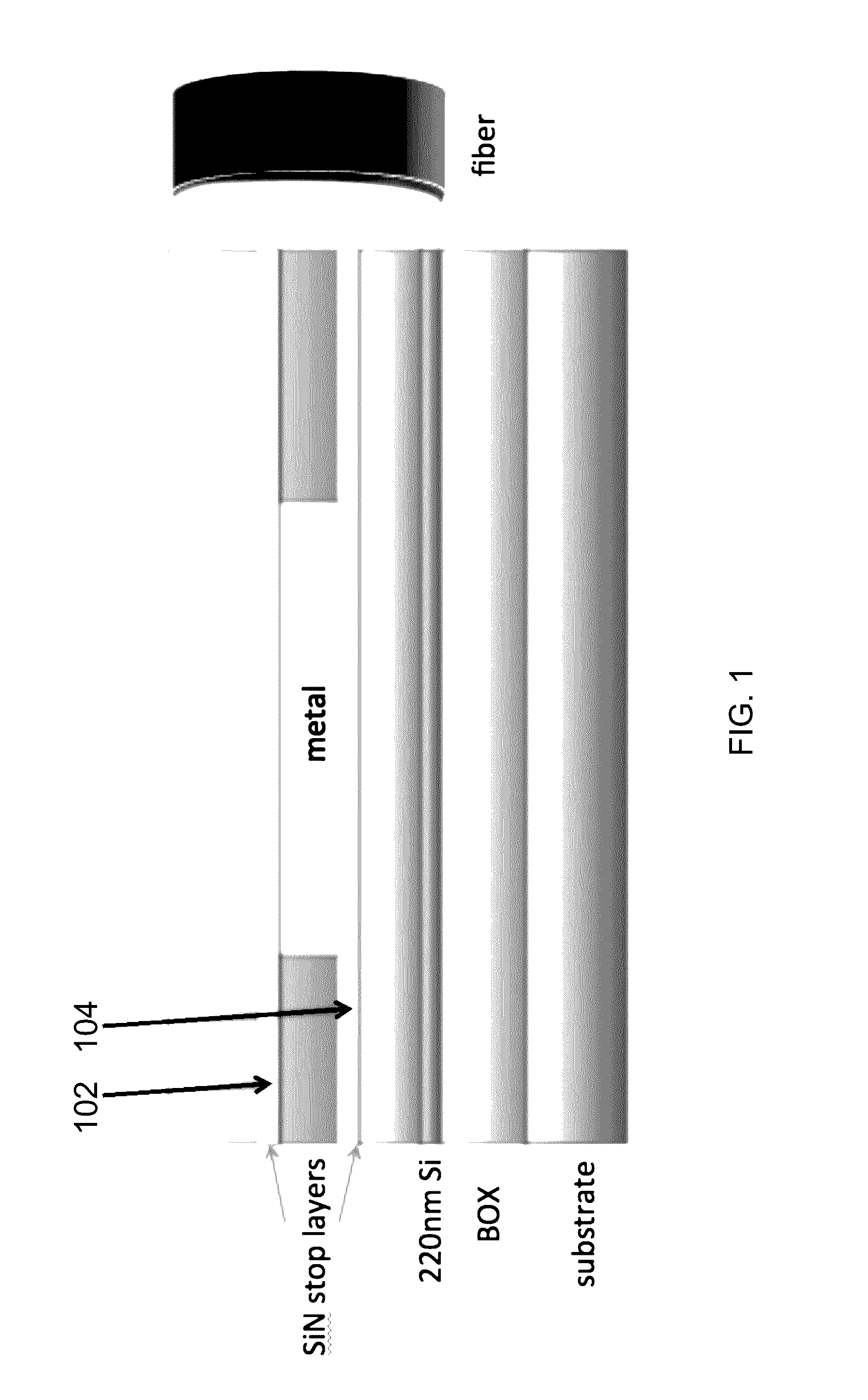
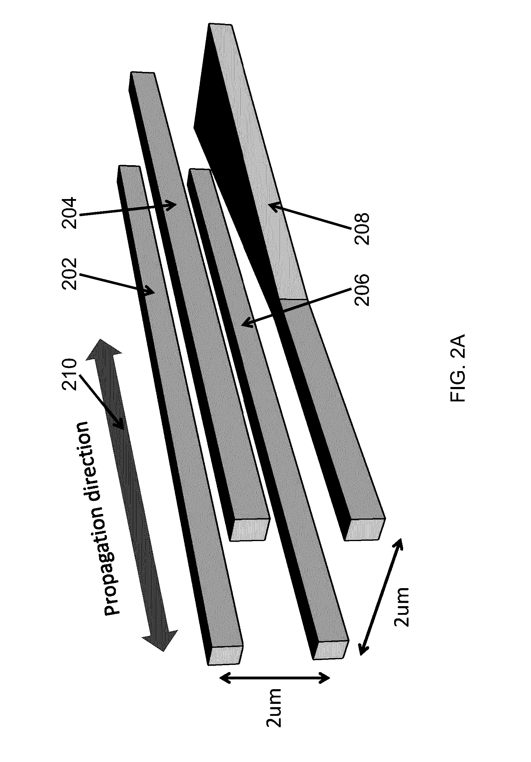
[0115]An embodiment of an edge coupler built using two SiN 102, 104 stop layers is designed for use with a standard single mode fiber. FIG. 2A is a perspective diagram of a composite waveguide having a group of waveguide cores according to the principles of the invention.
[0116]The thickness of each SiN layer is 120 nm, and the SiO2 between the two layers is 2 μm thick. On each layer, there are two SiN waveguide cores (202, 204) (206, 208) with 2 μm center-to-center separation, and the width of the waveguide cores are each 300 mm. As illustrated in FIG. 2A, the lower-right waveguide core 208 is used as output, and is tapered from 300 nm width×120 nm height to 1 μm width×120 nm height with a length of 100 μm.
[0117]In various embodiments, the width of the waveguide core used as the coupler may be varied, to see how the behavior changes with width. FIG. 3A-FIG. 3D are diagrams of mode profiles of the group of waveguide cores for selected widths of the edge coupler.
[0118]FIG. 2B is anoth...
PUM
 Abstract
Description
Claims
Application Information


