
Organic Light Emitting Display Device and Method for Manufacturing the Same

a technology of light-emitting display device and which is applied in the direction of solid-state device, sustainable manufacturing/processing, final product manufacturing, etc., can solve the problems of cracks and cracks in the anode, the flexibility of the transparent conductive oxide used as the anode of the organic light-emitting display element is lower than that of other materials in the active area, and the rectangular shape of the rectangular shape is vulnerable to tensil

Active Publication Date: 2016-12-08
LG DISPLAY CO LTD
View PDF1 Cites 2 Cited by
  • Summary
  • Abstract
  • Description
  • Claims
  • Application Information

AI Technical Summary

Benefits of technology

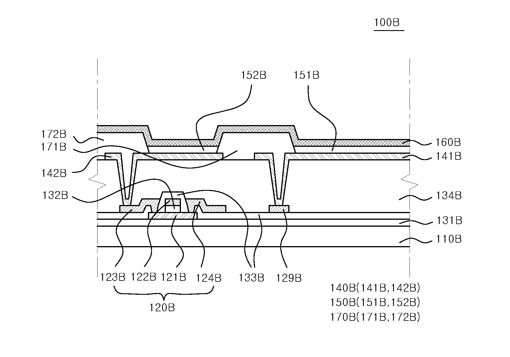
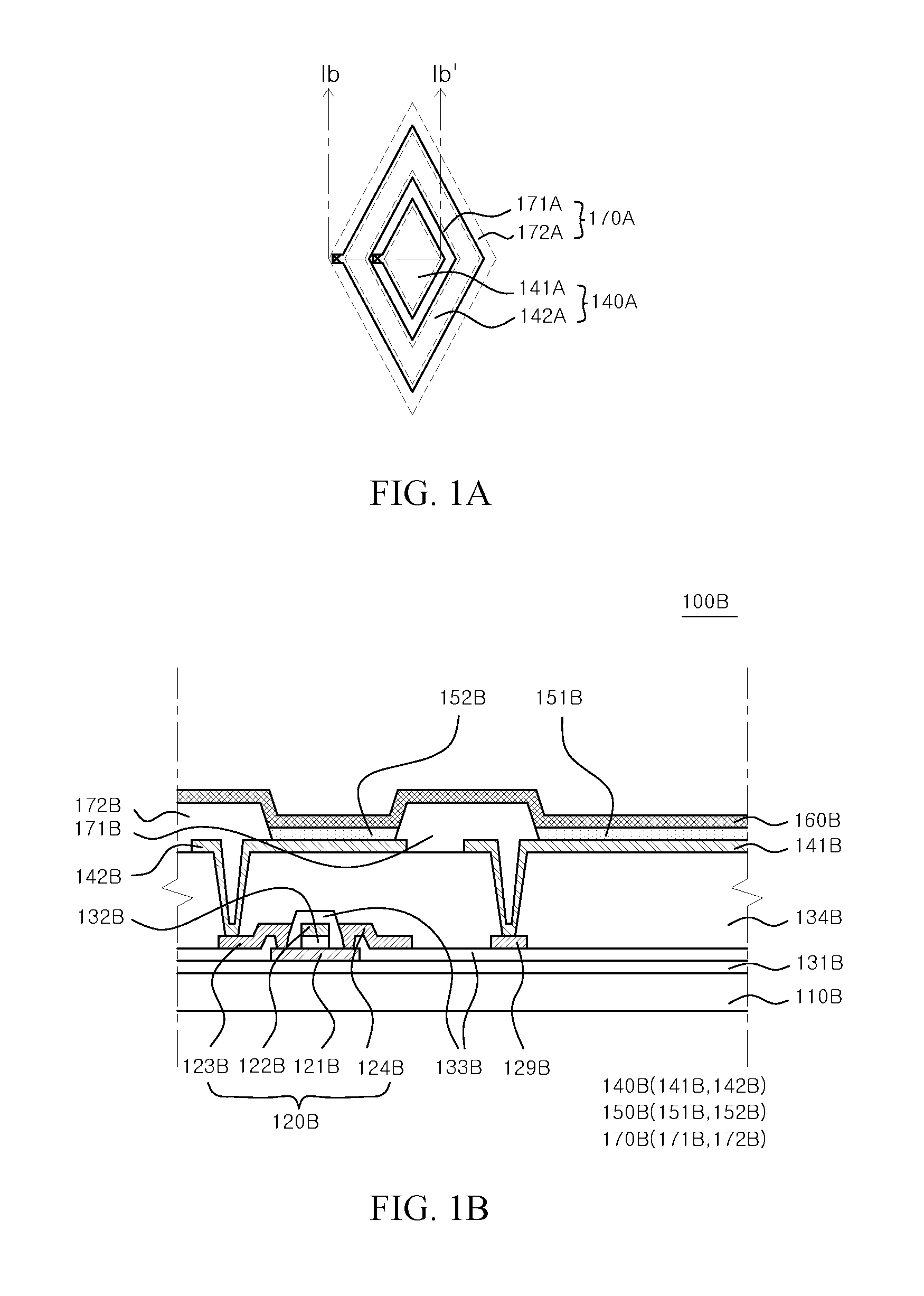
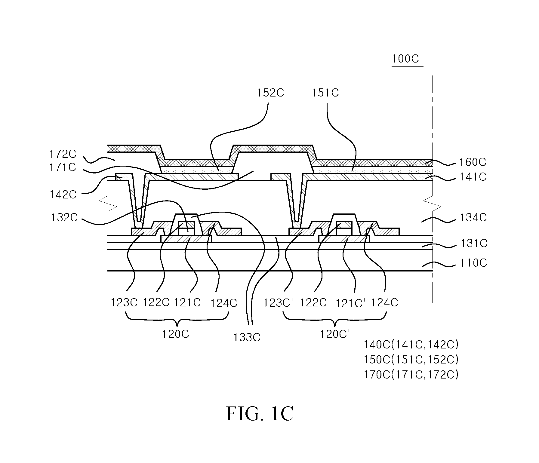
The present invention provides an organic light emitting display device with a new pixel configuration and anode structure that can withstand bending stress and minimize cracks in the anode. This reduces non-uniformity and prevents reduced luminance in the organic light emitting display element. The new anode structure includes a first anode, a second anode, and a third anode arranged in a triangular shape that disperses force and minimizes bending stress on the anode. The flexible organic light emitting display device with this new anode structure can be used for a variety of applications such as flexible displays, wearable displays, and displays for virtual reality devices.

Problems solved by technology

The anode in a rectangular shape is vulnerable to a tensile force and a compressive force in bending of the organic light emitting display device.
Further, a transparent conductive oxide used as the anode of the organic light emitting display device has lower flexibility as compared with other materials included in an active area where images are displayed.
Thus, cracks may occur in the anode when bending the active area where the organic light emitting display device is disposed.
With cracks in the anode, parts of the anode may be unable to receive the signal from the thin-film transistor.
This may result in reduced luminance in the organic light emitting display element.

Method used


Image

  • Organic Light Emitting Display Device and Method for Manufacturing the Same
  • Organic Light Emitting Display Device and Method for Manufacturing the Same
  • Organic Light Emitting Display Device and Method for Manufacturing the Same

Examples


Embodiment Construction

[0046]Various advantages and features of the present invention and methods accomplishing thereof will become apparent from the following description of embodiments with reference to the accompanying drawings. However, the present invention is not limited to exemplary embodiment disclosed herein but will be implemented in various forms. The exemplary embodiments are provided by way of example only so that a person of ordinary skilled in the art can fully understand the disclosures of the present invention and the scope of the present invention. Therefore, the present invention will be defined only by the scope of the appended claims.

[0047]Indicating that elements or layers are “on” other elements or layers include both a case in which the corresponding elements are just above other elements and a case in which the corresponding elements are intervened with other layers or elements.

[0048]Although first, second, and the like are used in order to describe various components, the compone...


PUM


Abstract

The organic light emitting display device includes a flexible substrate, a thin-film transistor on the flexible substrate, a first anode on the thin-film transistor, a second anode on the same plane with the first anode and spaced apart from the first anode so as to surround the first anode, an organic light emitting layer on the first anode and the second anode, and a cathode on the organic light emitting layer. The second anode includes an opening where the first anode is encompassed therein. The shape of the first anode and the second anode and arrangement thereof reduces a segment length of an anode in a bending direction of the organic light emitting display device, and, thus, occurrence of cracks in the anode can be minimized.

Description

CROSS-REFERENCE TO RELATED APPLICATIONS[0001]This application is a continuation of U.S. patent application Ser. No. 14 / 514,852 filed on Oct. 15, 2014, which claims the benefit of Republic of Korea Patent Application No. 10-2013-0130882 filed on Oct. 31, 2013, in the Korean Intellectual Property Office, the disclosure of both of which are herein incorporated by reference in their entirety.BACKGROUND[0002]Field of Technology[0003]The present disclosure relates to an organic light emitting display device and a method for improving flexibility of the organic light emitting display device. More particularly, the present disclosure relates to an organic light emitting display device and method for minimizing crack occurrences in an active area by reducing the strain on an organic light emitting element from the bending stress.[0004]Description of the Related Art[0005]In recent years, flexible display devices manufactured to display an image even when bent like paper by forming a display u...

Claims


Application Information

Patent Timeline
Patent Type & Authority Applications(United States)
IPC IPC(8): H01L27/32H01L51/00
CPCH01L27/3262H01L27/3246H01L27/3211H01L51/0097H01L27/322Y02E10/549Y02P70/50H10K59/123H10K77/111H10K2102/311H10K59/80515H10K59/80516H10K59/122H10K2102/302H10K59/1213H10K50/813H10K50/814H10K59/35H10K59/38
Inventor HA, ANNALEE, CHANWOOYOUN, SANGCHEON
Owner LG DISPLAY CO LTD
Learn More