

Plasma processing apparatus
a processing apparatus and plasma technology, applied in plasma techniques, electrical apparatus, electric discharge tubes, etc., can solve the problems of long maintenance time, heavy burden on workers, and inability to achieve the effect of reducing maintenance time and improving processing efficiency
- Summary
- Abstract
- Description
- Claims
- Application Information
AI Technical Summary
Benefits of technology
Problems solved by technology
Method used
Image

Examples
Embodiment Construction
[0034]An embodiment of the present invention will be described with reference to the drawings.
[0035]An example of the present invention will be described with reference to FIGS. 1 to 14. Identical reference signs in the drawings indicate identical components.
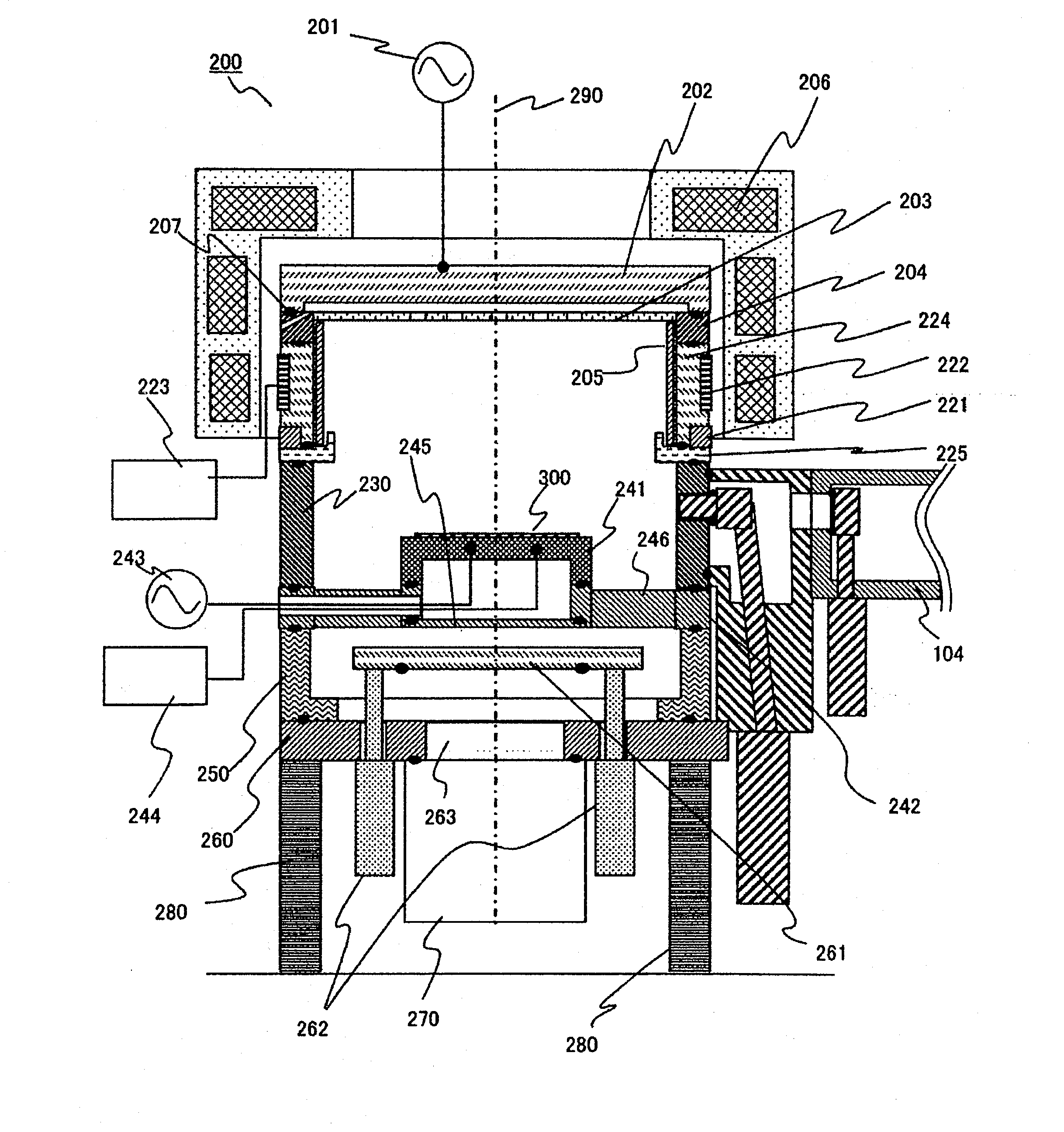
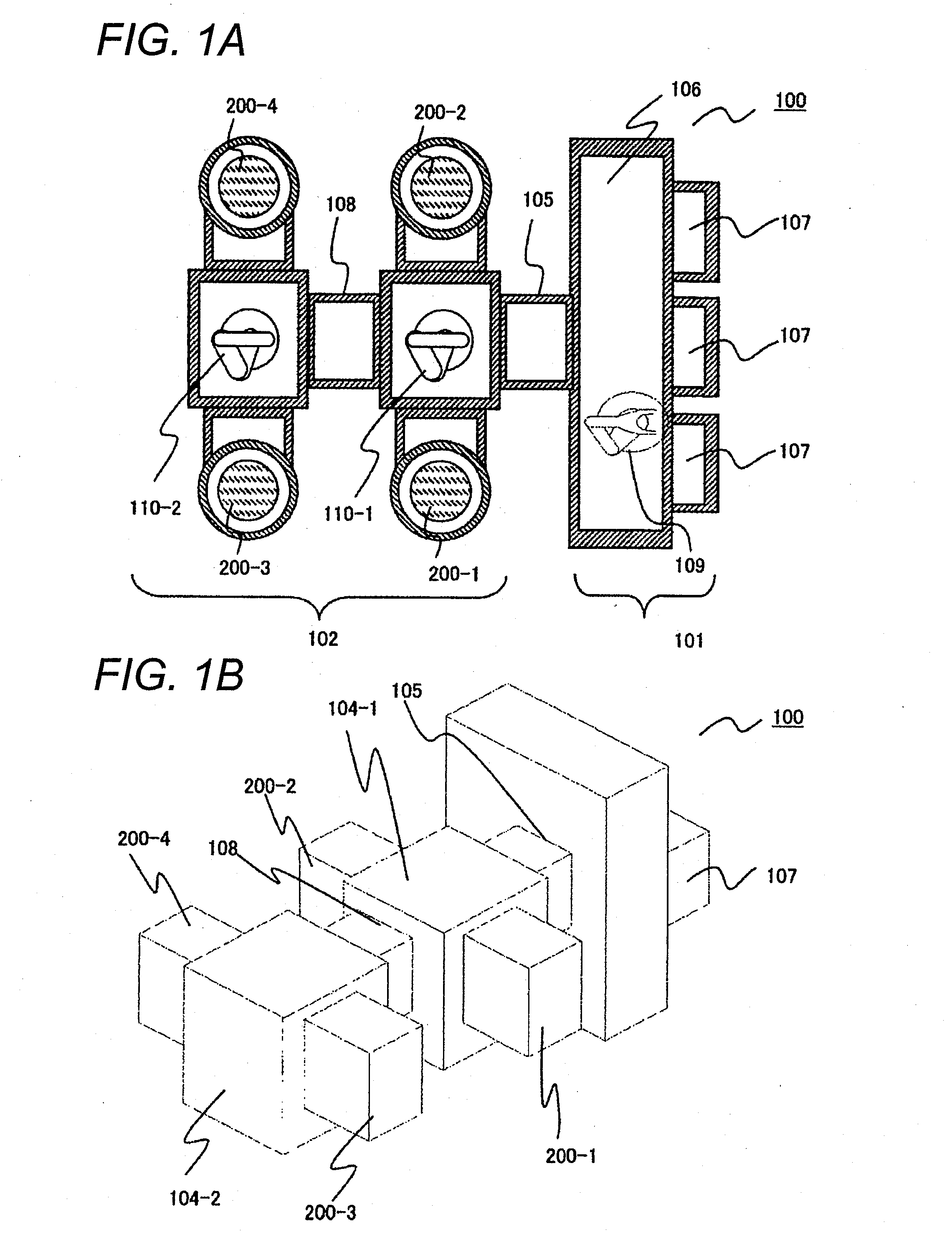
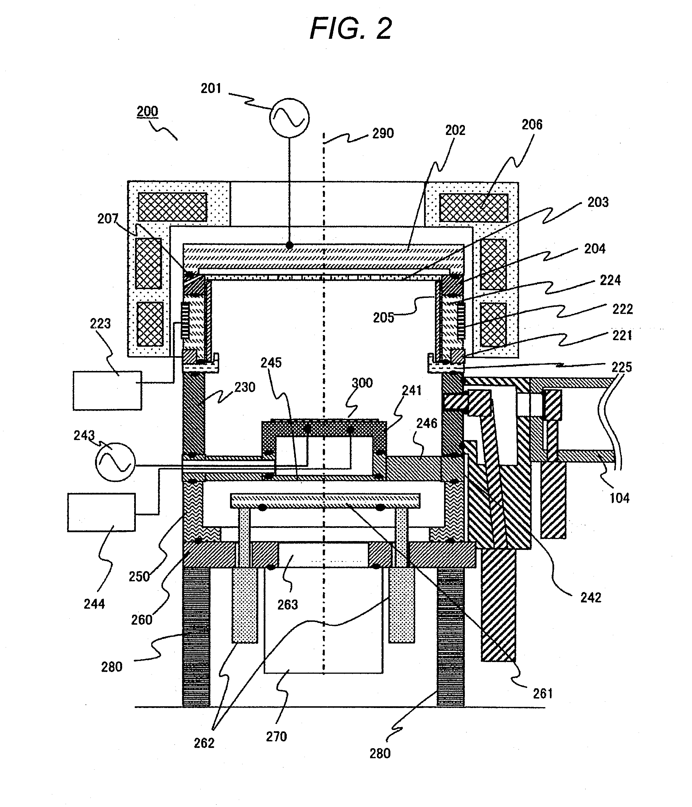
[0036]FIGS. 1A and 1B are diagrams illustrating schematically a configuration of a vacuum processing apparatus according to an example of the present invention. FIG. 1A is a transverse cross-sectional view of a vacuum processing apparatus 100 seen from above according to the example, and FIG. 1B is a perspective view of the vacuum processing apparatus 100 according to the example.
[0037]The vacuum processing apparatus 100 in the example includes an air block 101 arranged at the front side (the right side in FIGS. 1A and 1B) and a vacuum block 102 arranged at the rear side (the left side in FIGS. 1A and 1B). A substrate-like specimen such as a semiconductor wafer is transferred into the air block 101 and positioned there under air...
PUM
 Abstract
Description
Claims
Application Information