Thin film transistor substrate and display device using the same

a thin film transistor and substrate technology, applied in semiconductor devices, instruments, electrical devices, etc., can solve the problem that conventional display devices may have a limitation on low power consumption, and achieve the effect of improving image quality

Active Publication Date: 2016-12-22
LG DISPLAY CO LTD
View PDF11 Cites 71 Cited by
  • Summary
  • Abstract
  • Description
  • Claims
  • Application Information

AI Technical Summary

Benefits of technology

[0010]An advantage of the present invention is to provide a display device with improved image quality.
[0011]Additional features and advantages of the invention will be set forth in the description which follows, and in part will be apparent from the description, or may be learned by practice of the invention. These and other advantages of the invention will be realized and attained by the structure particularly pointed out in the written description and claims hereof as well as the appended drawings.
[0012]To achieve these and other advantages and in accordance with the purpose of the present invention, as embodied and broadly described, a thin film transistor substrate may, for example, include a first thin film transistor on a substrate and including a polycrystalline semiconductor layer, a first gate electrode, a first source electrode and a first drain electrode; a second thin film transistor separated from the first thin film transistor and including a second gate electrode, an oxide semiconductor layer, a second source electrode, and a second drain electrode that are disposed on a layer covering the first gate electrode; and a plurality of storage capacitors separated from the first and second thin film transistors, the plurality of storage capacitors each including a first dummy semiconductor layer, a first gate insulating layer on the first dummy semiconductor layer, a first dummy gate electrode on the first gate insulating layer, an intermediate insulating layer on the first dummy gate electrode, a second dummy gate electrode on the intermediate insulating layer, a second gate insulating layer on the second dummy...

Problems solved by technology

However, conventional display devices may have a limitation on low power consump...

Method used


Image

  • Thin film transistor substrate and display device using the same
  • Thin film transistor substrate and display device using the same
  • Thin film transistor substrate and display device using the same

Examples


first embodiment

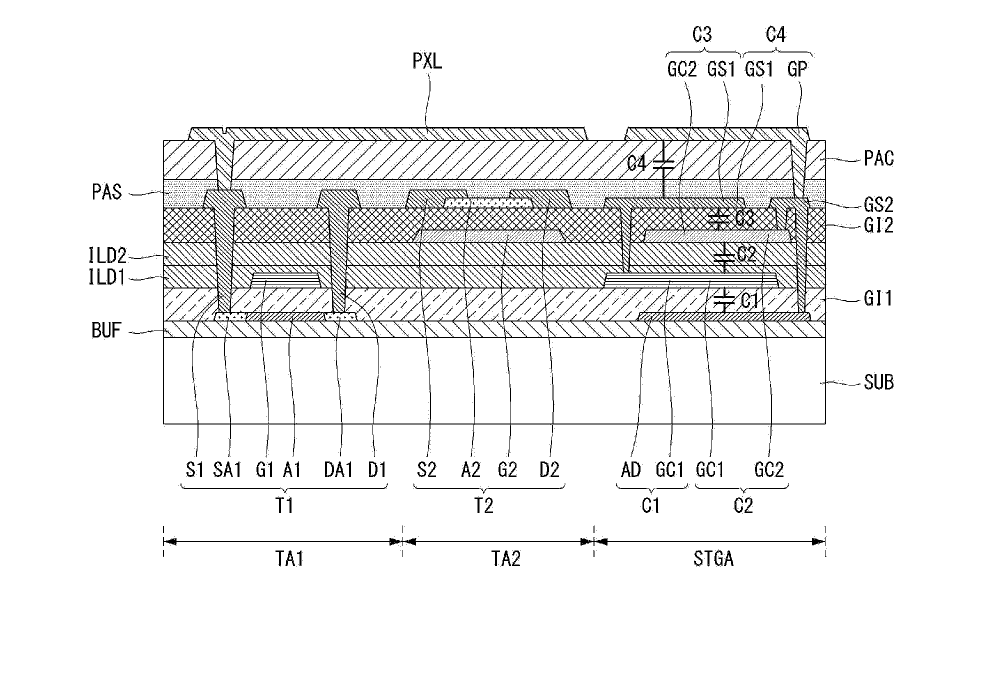
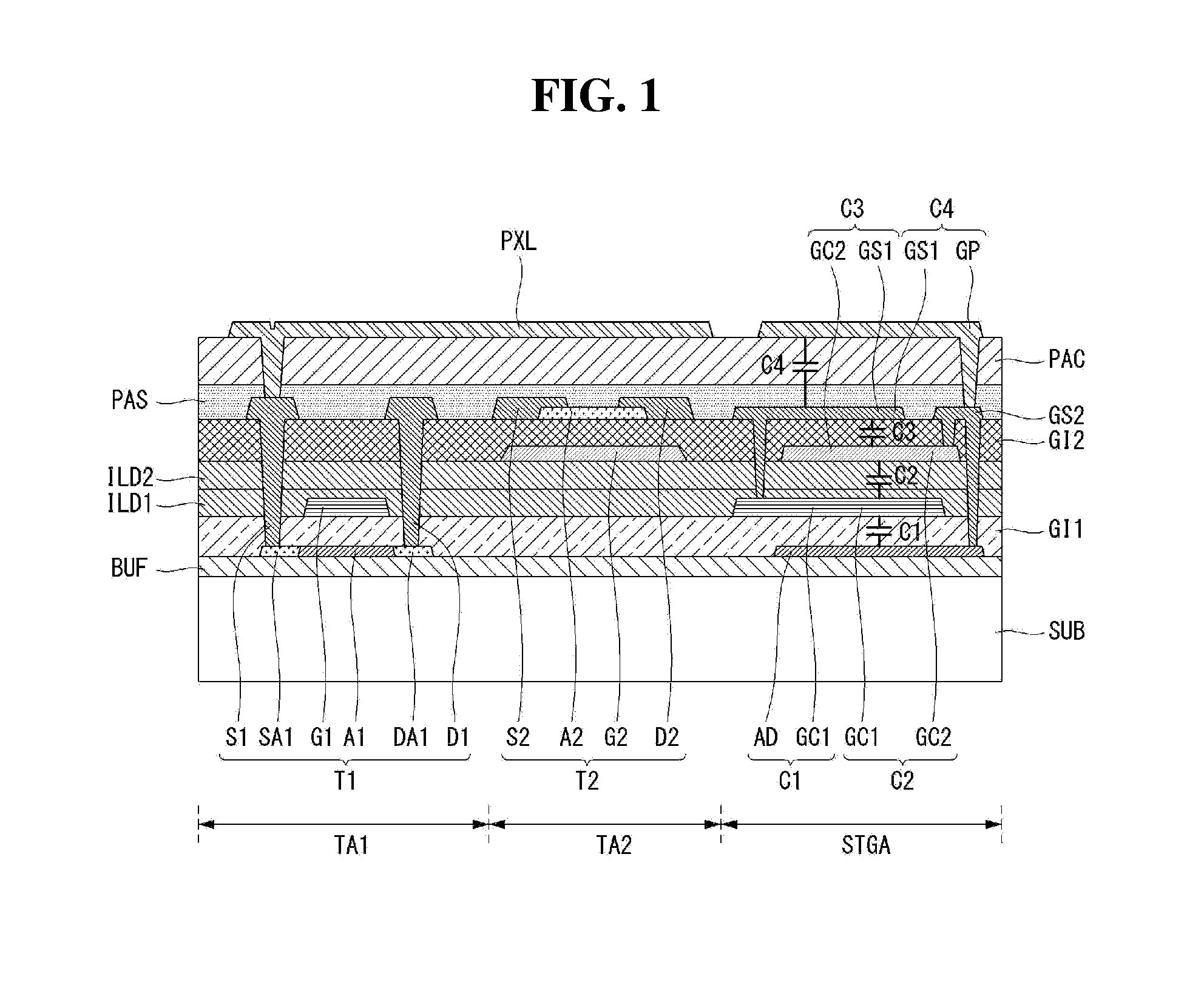
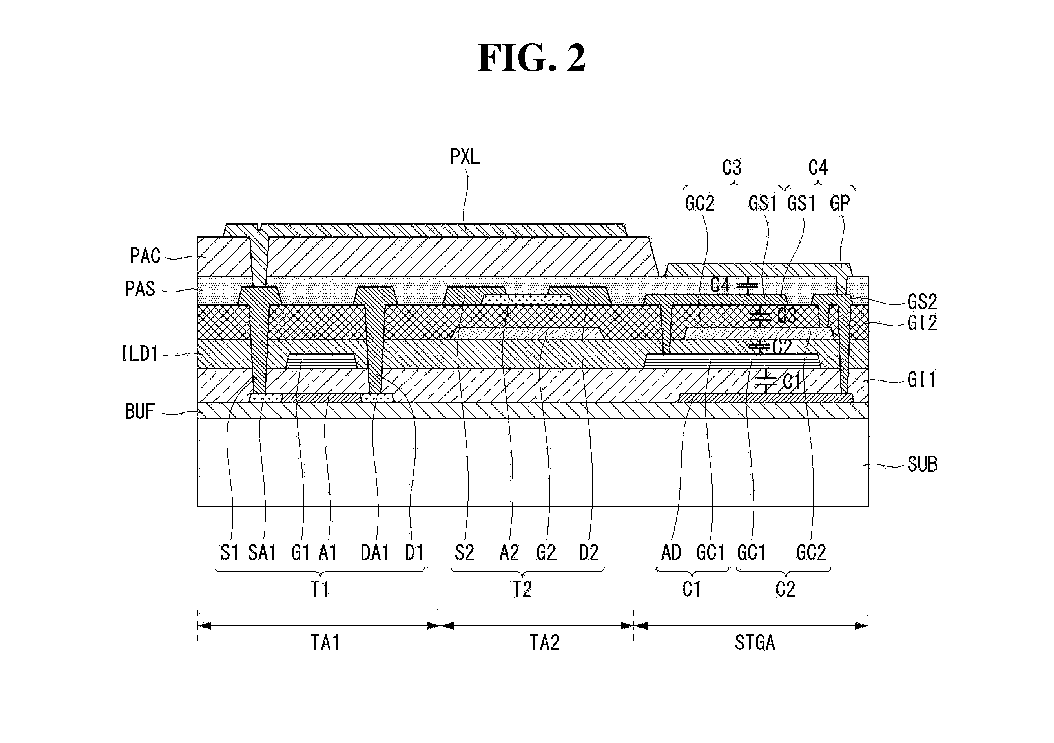
[0037]FIG. 1 is a cross-sectional view illustrating a thin film transistor (TFT) substrate for a display device including different types of TFTs according to the first embodiment of the present disclosure. FIG. 2 is a cross-sectional view illustrating a modified example of FIG. 1. In the embodiment disclosed herein, a cross-sectional view of a portion of the TFT substrate is illustrated for the sake of brevity and ease of understanding.

[0038]Referring to FIG. 1, the TFT substrate for a display device according to the first embodiment of the present disclosure includes a first TFT T1 and a second TFT T2 that are disposed on a substrate SUB, and first to fourth storage capacitors C1 to C4. The first TFT T1 and the second TFT T2 may be separated from each other at a predetermined distance.

[0039]A buffer layer BUF is formed on an entire surface of the substrate SUB. The buffer layer BUF may have a single-layered structure including silicon nitride (SiNx) or silicon oxide (SiOx) or a mu...

second embodiment

[0070]FIG. 3 is a cross-sectional view illustrating a TFT substrate for a display device including different types of TFTs according to the second embodiment of the present disclosure. FIG. 4 is a cross-sectional view illustrating a modified example of FIG. 3. In the embodiment disclosed herein, a cross-sectional view of a portion of the TFT substrate is illustrated for the sake of brevity and ease of understanding.

[0071]Referring to FIG. 3, the TFT substrate for a display device according to the second embodiment of the present disclosure includes a first TFT T1 and a second TFT T2 that are disposed on a substrate SUB, and first to third storage capacitors C1 to C3. The first TFT T1 and the second TFT T2 may be separated from each other at a predetermined distance.

[0072]A buffer layer BUF is formed on an entire surface of the substrate SUB. The buffer layer BUF may have a single-layered structure including silicon nitride (SiNx) or silicon oxide (SiOx) or a multi-layered structure ...

third embodiment

[0098]FIG. 5 is a cross-sectional view illustrating a TFT substrate for a display device including different types of TFTs according to the third embodiment of the present disclosure. FIG. 6 is a cross-sectional view illustrating a modified example of FIG. 5. In the embodiment disclosed herein, a cross-sectional view of a portion of the TFT substrate is illustrated for the sake of brevity and ease of understanding.

[0099]Referring to FIG. 5, the TFT substrate for display device according to the third embodiment of the present disclosure includes a first TFT T1 and a second TFT T2 that are disposed on a substrate SUB, and first to fourth storage capacitors C1 to C4. The first TFT T1 and the second TFT T2 may be separated from each other at a predetermined distance.

[0100]A buffer layer BUF is formed on an entire surface of the substrate SUB. The buffer layer BUF may have a single-layered structure including silicon nitride (SiNx) or silicon oxide (SiOx) or a multi-layered structure inc...


PUM


Abstract

A thin film transistor (TFT) substrate and a display device using the same are disclosed. The TFT substrate includes a first TFT including a polycrystalline semiconductor layer, a first gate electrode, a first source electrode, and a first drain electrode deposited on a substrate, a second TFT separated from the first TFT, the second TFT including a second gate electrode, an oxide semiconductor layer, a second source electrode, and a second drain electrode deposited on the first gate electrode, and a plurality of storage capacitors separated from the first and second TFTs, each storage capacitor including a first dummy semiconductor layer, a first gate insulating layer on the first dummy semiconductor layer, a first dummy gate electrode on the first gate insulating layer, and an intermediate insulating layer on the first dummy gate electrode.

Description

[0001]This application claims the benefit of Korean Patent Application No. 10-2015-0087209 filed on Jun. 19, 2015, which is incorporated herein by reference for all purposes as if fully set forth herein.BACKGROUND OF THE INVENTION[0002]Field of the Invention[0003]The present disclosure relates to a display device and a method of manufacturing the same. More particularly, the present disclosure relates to a display device including a thin film transistor (TFT) substrate.[0004]Discussion of the Related Art[0005]As information society is developed, display devices for representing information are in demand. A field of display devices has rapidly changed from large-sized cathode ray tubes (CRTs) to flat panel displays (FPDs) which have advantageous characteristics of thin profile and lightweight and can be implemented into a large-sized screen. Examples of flat panel displays include liquid crystal displays (LCDs), plasma display panels (PDPs), organic light emitting diode (OLED) displa...

Claims


Application Information

Patent Timeline
IPC IPC(8): H01L27/12G02F1/1343G02F1/1362G02F1/1333H01L27/32G02F1/1368
CPCH01L27/1255H01L27/1222H01L27/124H01L27/3211H01L27/3246H01L27/3248G02F2001/134372G02F1/136213G02F1/133345G02F1/134309G02F1/136227G02F2001/133357G02F1/1368H01L27/1214H10K59/12H01L27/1225H01L27/1251G02F1/134372H10K59/1216H10K59/38
Inventor LEE, SOHYUNGCHANG, YOUNGYOUNGPARK, KWONSHIKKIM, MINCHEOLYANG, JEONGSUK
Owner LG DISPLAY CO LTD
Why Eureka
Try Eureka