Gate driving circuit and a driving method thereof, as well as a display device

a driving circuit and driving method technology, applied in the field of display technology, can solve problems such as insufficient charging rate and defects of dark or bright lines, and achieve the effects of improving dark or bright line defects, avoiding insufficient charging rate of rows, and high report ra

Active Publication Date: 2017-01-12
BOE TECH GRP CO LTD
View PDF1 Cites 40 Cited by
  • Summary
  • Abstract
  • Description
  • Claims
  • Application Information

AI Technical Summary

Benefits of technology

[0008]The embodiment of the present invention provides a gate driving circuit and a driving method thereof, as well as a display device, which can avoid insufficient charging rate of the row of pixels, and improve dark or bright line defects.
[0019]The gate driving circuit and the driving method thereof, as well as the display device provided by the embodiment of the present invention, by additionally arranging a pre-charging unit connected with the corresponding first stage of shift register unit when the gate row drive scanning is performed again after the touch control scanning is accomplished, can pre-charge the first stage of shift register unit during the touch control scanning. In this way, the electric leakage phenomenon of the pull-up control node (PU point) of the corresponding first stage of shift register unit when the gate row drive scanning is performed again after the touch control scanning is accomplished due to a relatively long touch control scanning time interval between output of two rows of shift register units is avoided, thereby avoiding the defect of insufficient charging rate of row of pixels while ensuring touch control scanning of high report rate, which improves dark or bright line defects significantly and increases the display quality.

Problems solved by technology

Since a relatively long scanning time exists between the outputs of the N / 2 row and the N / 2+1 row, electric leakage may occur to the potential of the PU point through the connected TFT, thereby affecting the pre-charging of the shift register unit of the N / 2+1 row seriously, such that the voltage will be reduced when the shift register unit of the N / 2+1 row performs output, thereby resulting in insufficient charging rate of the pixels of this row, and the defect of dark or bright line may occur.

Method used


Image

  • Gate driving circuit and a driving method thereof, as well as a display device
  • Gate driving circuit and a driving method thereof, as well as a display device
  • Gate driving circuit and a driving method thereof, as well as a display device

Examples


Embodiment Construction

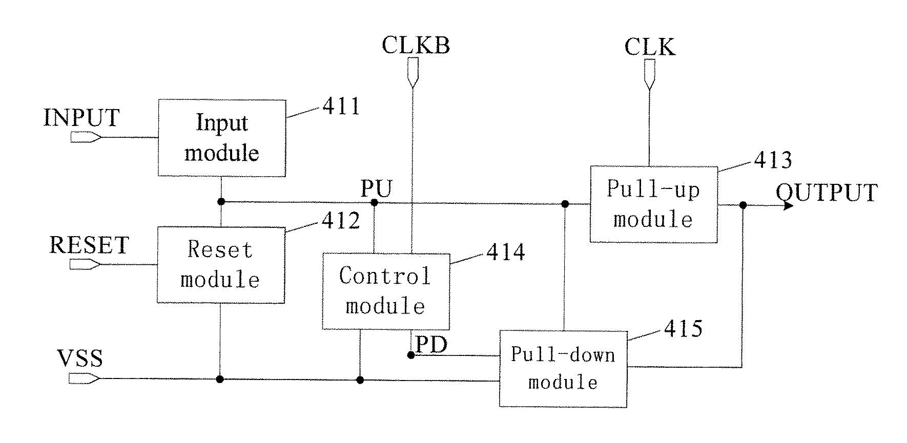
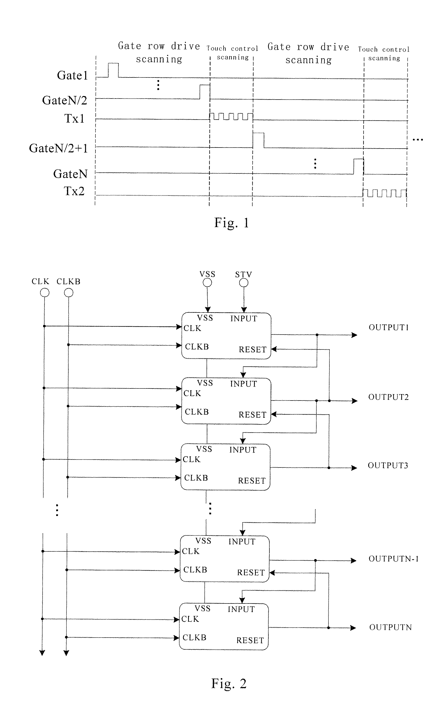
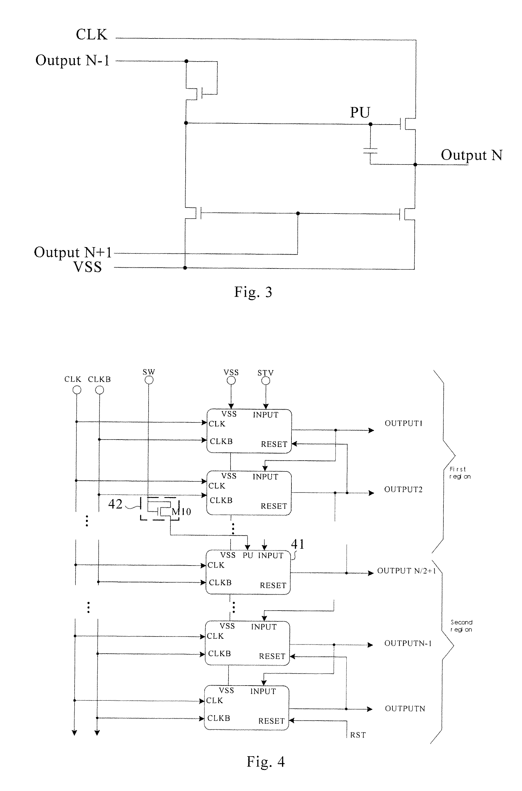
[0028]Next, the technical solutions in embodiments of the present invention will be described clearly and completely by combining the drawings in embodiments of the present invention, apparently, the embodiments described are only part rather than all of the embodiments of the present invention. All the other embodiments obtained by the ordinary skilled person in the art based on the embodiments in the present invention belong to the protection scope of the present invention.

[0029]The transistors used in all the embodiments of the present invention may be thin film transistors or field effect transistors or other devices with the same characteristics. Since the source and the drain of the transistor used here are symmetric, its source and drain are the same from the perspective of the structure of the device. In the embodiments of the present invention, in order to distinguish the two poles other than the gate of the transistor, one pole thereof is called a first pole, and the other...


PUM


Abstract

The present invention provides a gate driving circuit and a driving method thereof, a display device, which relates to the field of display technology. The gate driving circuit may comprise a plurality of mutually cascaded shift register units and a pre-charging unit, the gate row drive scanning and touch control scanning of the plurality of mutually cascaded shift register units are performed alternately. By additionally arranging a pre-charging unit connected with the corresponding first stage of shift register unit when the gate row drive scanning is performed again after the touch control scanning is accomplished, the first stage of shift register unit can be pre-charged during the touch control scanning. In this way, the electric leakage phenomenon of the pull-up control node (PU point) of the corresponding first stage of shift register unit when the gate row drive scanning is performed again after the touch control scanning is accomplished due to a relatively long touch control scanning time interval between outputs of two rows of shift register units is avoided, thereby avoiding the defect of insufficient charging rate of row of pixels while ensuring touch control scanning of high report rate.

Description

FIELD OF THE INVENTION[0001]The present invention relates to the field of display technology, particularly to a gate driving circuit and a driving method thereof, as well as a display device.BACKGROUND OF THE INVENTION[0002]With the growing popularization of touch control display devices, people's requirement on quality of the touch control display devices becomes higher and higher. The in-cell touch technology has been widely used for its advantages of reduced thickness and high touch sensitivity and the like.[0003]The in-cell touch technology, i.e., the touch control element, is integrated in the display panel, so that the panel itself has the touch function, and the touch effect and application can be achieved without fitting and assembling with the touch panel additionally. Taking the typical thin film transistor-liquid crystal display (TFT-LCD) as the example, its characteristic is that the manufacture of the touch sensing element is accomplished in the standard manufacturing p...

Claims


Application Information

Patent Timeline
Patent Type & Authority Applications(United States)
IPC IPC(8): G06F3/041G06F3/044G09G3/36
CPCG06F3/0416G06F3/0412G06F2203/04104G06F3/044G09G2310/0286G09G3/3677G06F3/04184G09G3/20G09G2310/065G11C19/28G06F3/041G06F3/04166
Inventor ZHANG, YUANBOZHAO, JIAYANGHAN, SEUNGWOOZOU, XIANGXIANG
Owner BOE TECH GRP CO LTD
Why Eureka
Try Eureka