Multiple quantum well structure and method for manufacturing the same

Active Publication Date: 2017-02-02
GENESIS PHOTONICS
View PDF3 Cites 15 Cited by
  • Summary
  • Abstract
  • Description
  • Claims
  • Application Information

AI Technical Summary

Benefits of technology

[0007]The invention provides a multiple quantum well structure

Problems solved by technology

Accordingly, epitaxial defects are usually caused, leading to damage to the multi

Method used


Image

  • Multiple quantum well structure and method for manufacturing the same
  • Multiple quantum well structure and method for manufacturing the same
  • Multiple quantum well structure and method for manufacturing the same

Examples


Embodiment Construction

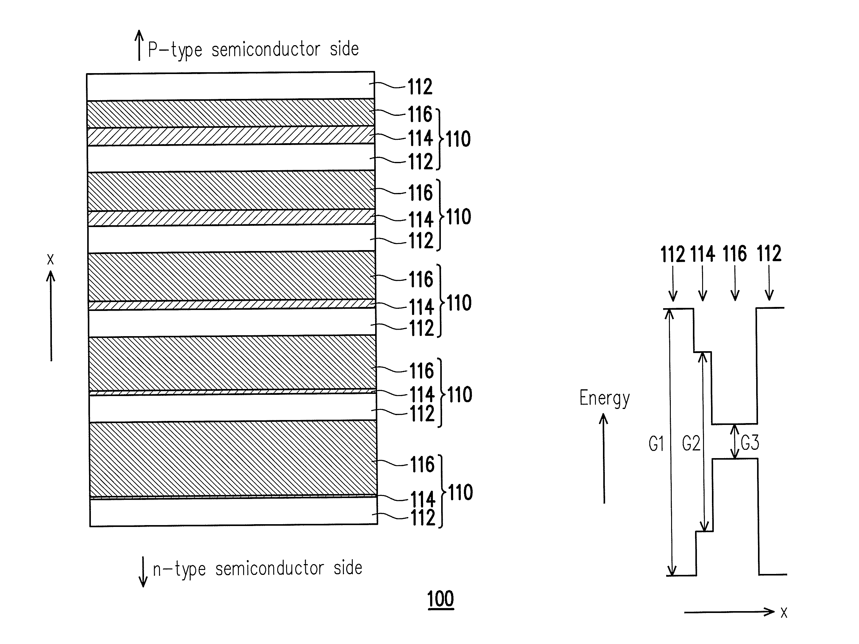
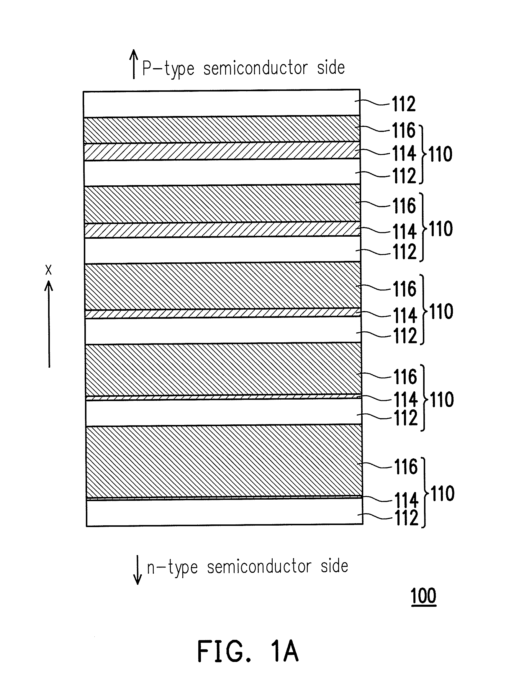
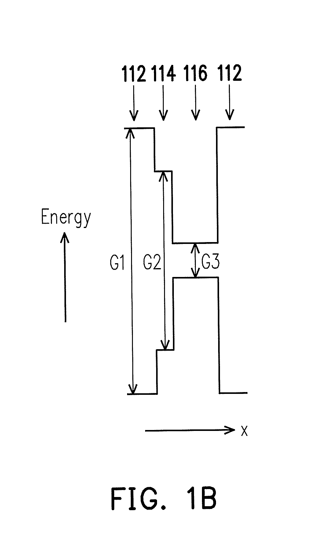
[0023]FIG. 1A is a schematic structural view of a multiple quantum well structure according to an embodiment of the invention. FIG. 1B is a band diagram corresponding to a well-barrier set of the multiple quantum well structure in FIG. 1A. Referring to FIGS. 1A and 1B, a multiple quantum well structure 100 in this embodiment includes a plurality of well-barrier sets 110 arranged along a direction x. Each of the well-barrier sets 110 includes a barrier layer 112, at least one intermediate level layer 114, and a well layer 116. The intermediate level layer 114 is beside the barrier layer 112, and the well layer 116 is beside the intermediate level layer 114. A bandgap G1 of the barrier layer 112 is greater than an average bandgap G2 of the intermediate level layer 114, and the average bandgap G2 of the intermediate level layer 114 is greater than a bandgap G3 of the well layer 116. The barrier layers 112, the intermediate level layers 114, and the well layers 116 of the well-barrier s...


PUM


Abstract

A multiple quantum well structure includes a plurality of well-barrier sets arranged along a direction. Each of the well-barrier sets includes a barrier layer, at least one intermediate level layer, and a well layer. A bandgap of the barrier layer is greater than an average bandgap of the intermediate level layer, and the average bandgap of the intermediate level layer is greater than a bandgap of the well layer. The barrier layers, the intermediate level layers, and the well layers of the well-barrier sets are stacked by turns. Thicknesses of at least parts of the well layers in the direction gradually decrease along the direction, and thicknesses of at least parts of the intermediate level layers in the direction gradually increase along the direction. A method for manufacturing a multiple quantum well structure is also provided.

Description

BACKGROUND OF THE INVENTION[0001]Field of the Invention[0002]The invention relates to a quantum well structure and a method for manufacturing the same, and more particularly, to a multiple quantum well structure and a method for manufacturing the same.[0003]Description of Related Art[0004]When material dimensions are reduced to nanometer scale, not only the dimensions are considerably miniaturized, but also some quantum effects such as confinement effects, surface and interface effects, and tunneling effects become particularly apparent. These characteristics may be applied to electronic component development, biochip fabrication, sensitivity enhancement of medical instruments, and so on.[0005]More specifically, due to particle and wave nature of electrons, in a nanomaterial, a length of an electron wave function is close to a feature size of a quantum structure, and the wave nature of electrons is sufficiently shown. Therefore, when a material is reduced to nanometer scale in a dir...

Claims


Application Information

Patent Timeline
IPC IPC(8): H01L33/06H01L33/32H01L33/00
CPCH01L33/002H01L33/32H01L33/0075H01L33/06H01L33/04H01L33/007
Inventor HUANG, CHI-FENGFANG, HSIN-CHIAOCHENG, CHI-HAO
Owner GENESIS PHOTONICS
Why Eureka
Try Eureka