Circuit board and manufacturing method thereof

a technology of circuit boards and manufacturing methods, applied in the field of circuit boards, can solve the problems of oxidizing or eroded conductive bumps, yield of chip package products, etc., and achieve the effect of better manufacturing precision

Active Publication Date: 2017-02-09
UNIMICRON TECH CORP
View PDF1 Cites 4 Cited by
  • Summary
  • Abstract
  • Description
  • Claims
  • Application Information

AI Technical Summary

Benefits of technology

[0006]Accordingly, the invention is directed to a circuit board and a manufacturing method thereof, in which conductive bu...

Problems solved by technology

However, since the conductive bumps are required to have a higher height, side surfaces of the conductive bumps are liable to be excessively expo...

Method used


Image

  • Circuit board and manufacturing method thereof
  • Circuit board and manufacturing method thereof
  • Circuit board and manufacturing method thereof

Examples


Embodiment Construction

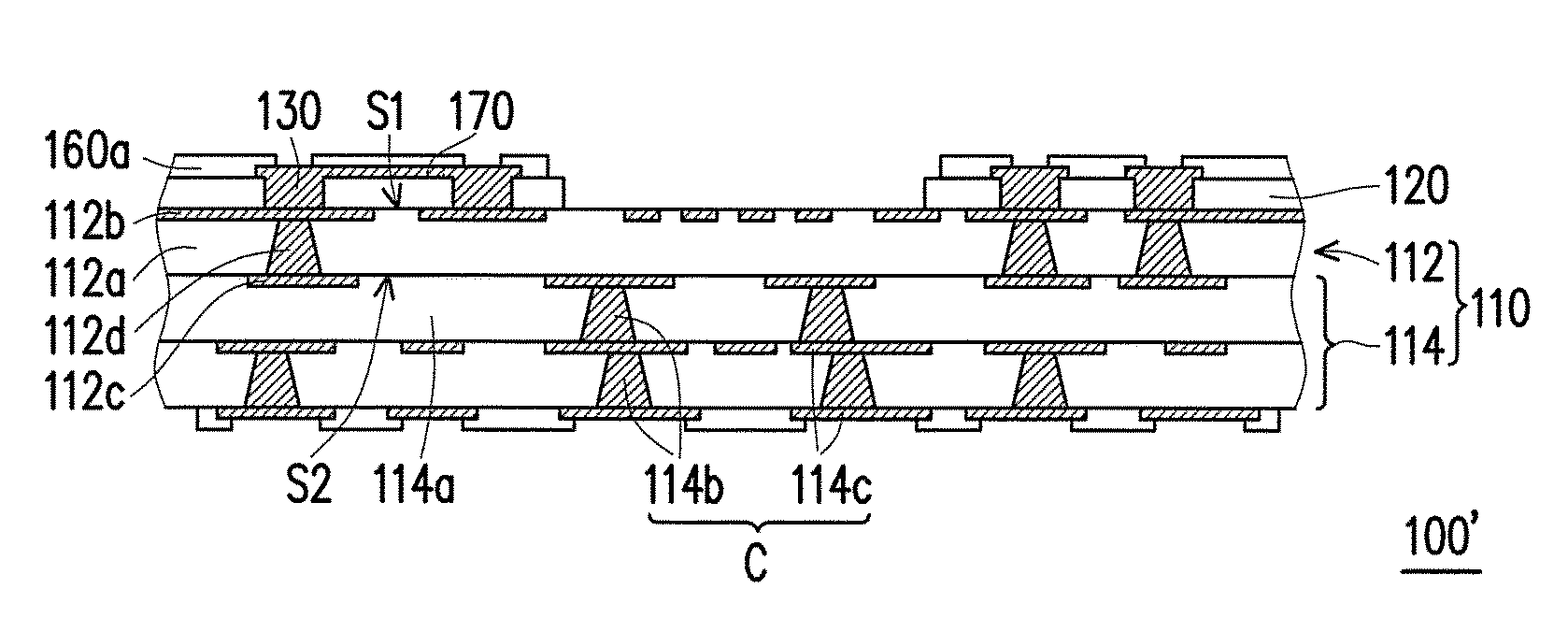
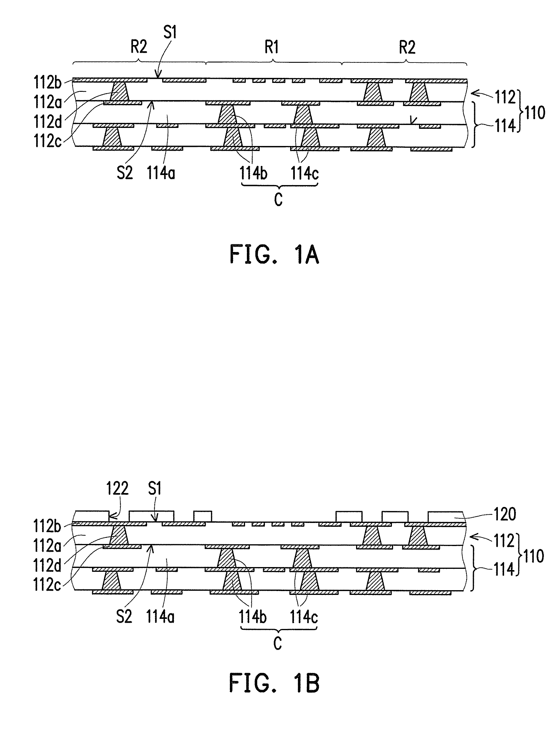
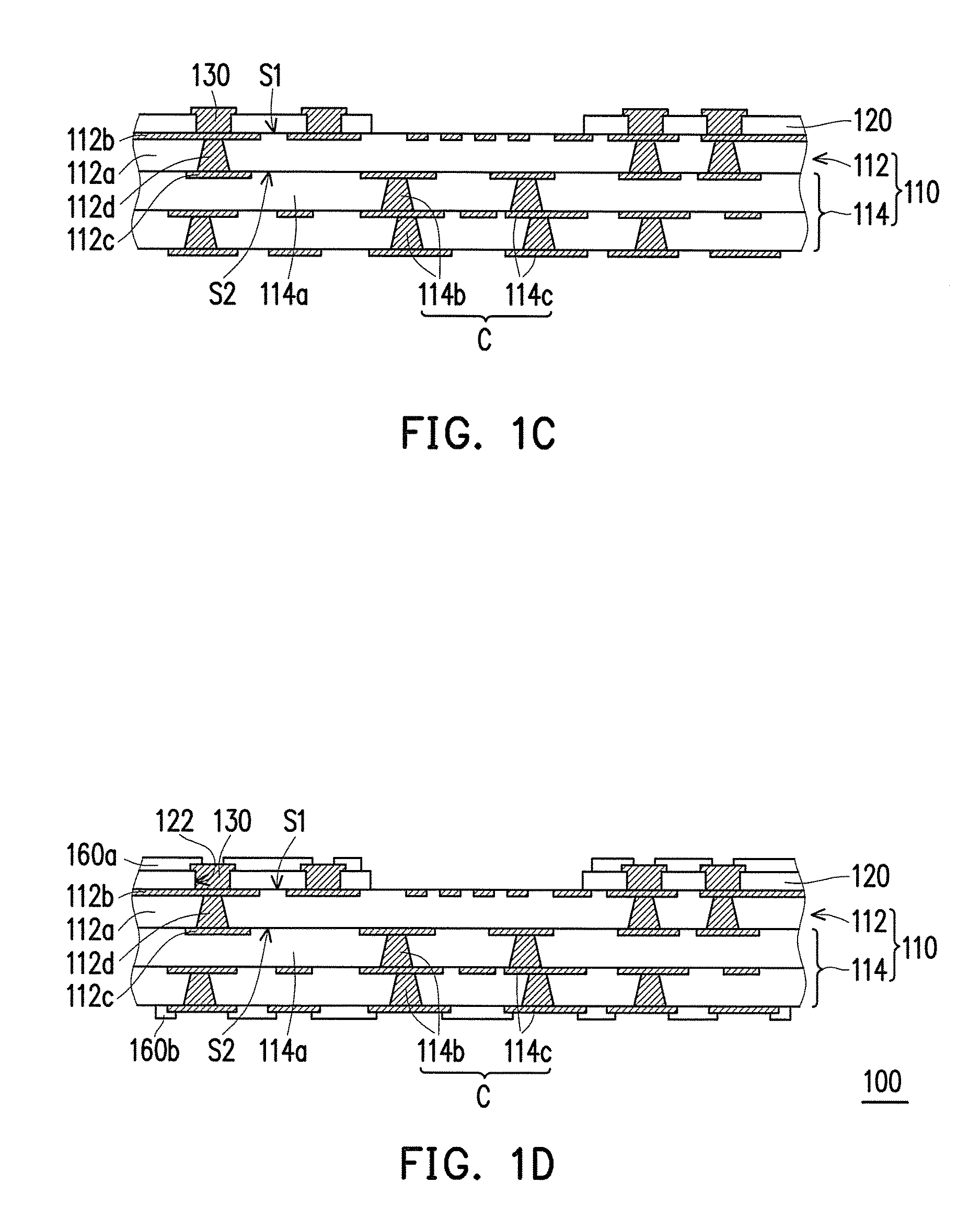
[0026]FIG. 1A to FIG. 1D illustrate a manufacturing flow of a circuit board according to an embodiment of the invention. Referring to FIG. 1A first, a substrate 110 is provided, the substrate 110 has a first surface S1 and a first circuit layer 112b, where the first surface S1 has a chip disposing area R1 and an electrical connection area R2 surrounding the chip disposing area R1, and the first circuit layer 112b is embedded in the first surface S1.

[0027]Then, as shown in FIG. 1B, a photo imageable dielectric layer 120 is formed on the electrical connection area R2, where the photo imageable dielectric layer 120 has a plurality of openings 122, and the openings 122 expose parts of the first circuit layer 112b. Then, as shown in FIG. 1C, a plurality of conductive bumps 130 is respectively formed on the electrical connection area R2 (indicated in FIG. 1A) through the openings 122, where each of the conductive bumps 130 is connected to the first circuit layer 112b, and the photo imagea...


PUM


Abstract

A circuit board including a substrate, a photo imageable dielectric layer and a plurality of conductive bumps is provided. The substrate has a first surface and a first circuit layer, wherein the first surface has a chip disposing area and an electrical connection area, and the first circuit layer is embedded in the first surface. The photo imageable dielectric layer is disposed on the electrical connection area and has a plurality of openings, wherein parts of the first circuit layer is exposed by the openings. The conductive bumps are disposed at the openings respectively and connected to the first circuit layer, wherein a side surface of each of the conductive bumps is at least partially covered by the photo imageable dielectric layer. In addition, a manufacturing method of the circuit board is also provided.

Description

BACKGROUND OF THE INVENTION[0001]Field of the Invention[0002]The invention relates to a circuit board and a manufacturing method thereof, and particularly relates to a circuit board having a photo imageable dielectric layer and a manufacturing method thereof.[0003]Description of Related Art[0004]Along with quick development of technology, integrated circuits (ICs) are widely applied in people's daily life. Generally, production of the ICs mainly includes three stages: manufacturing of silicon wafers, manufacturing of the ICs and packaging of the ICs. In view of a present package structure, package on package (POP) is a commonly used package type.[0005]To be specific, a chip package is fixed on another chip package through a plurality of conductive bumps, and is electrically connected to the other chip package through the conductive bumps. In recent years, as the number of input / output (I / O) terminals required on a circuit board is gradually increased, a layout density of the conduct...

Claims


Application Information

Patent Timeline
IPC IPC(8): H05K1/11H05K3/40H05K3/00H05K1/02H05K3/10
CPCH05K1/116H05K1/0298H05K3/10H05K2203/0562H05K3/4007H05K2201/0367H05K3/0023H05K1/111H05K1/113H05K3/0097H05K3/3452H05K3/4682H05K3/4697H05K2201/094H05K2201/09472H05K2203/1536Y02P70/50H05K1/119H05K3/303
Inventor WU, KUAN-HSIPAN, PI-TECHEN, CHANG-FU
Owner UNIMICRON TECH CORP
Why Eureka
Try Eureka