Wafer processing method

Active Publication Date: 2017-02-23
DISCO CORP
View PDF2 Cites 11 Cited by
  • Summary
  • Abstract
  • Description
  • Claims
  • Application Information

AI Technical Summary

Benefits of technology

[0008]According to the above method of laying the die-bonding resin in the “dicing before grinding” step, it is necessary to cut the die-bonding resin film applied to the reverse side of the wafer apart from dividing the wafer into the individual device chips, so that the entire step will be relatively complex. Moreover, the projected division lines after the wafer is divided into the individual semiconductor device chips subsequently to the grinding of the reverse side afte

Problems solved by technology

According to the above method of laying the die-bonding resin in the “dicing before grinding” step, it is necessary to cut the die-bonding resin film applied to the reverse side of the wafer apart from dividing the wafer into the individual device

Method used


Image

  • Wafer processing method
  • Wafer processing method
  • Wafer processing method

Examples


Embodiment Construction

[0027]A method of processing a wafer according to a preferred embodiment of the present invention will be described in detail below with reference to the accompanying drawings.

(Protective Member Placing Step)

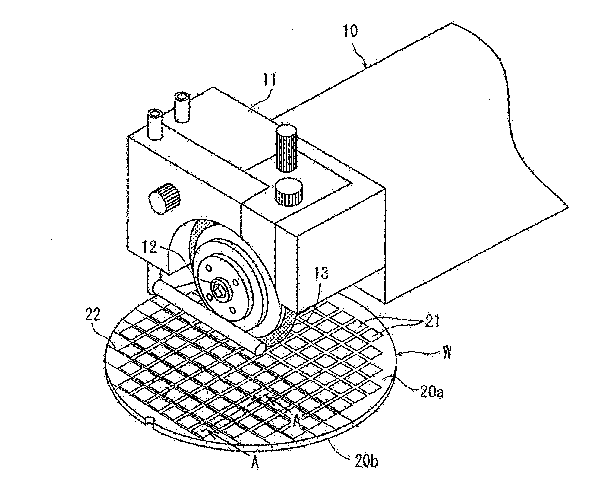
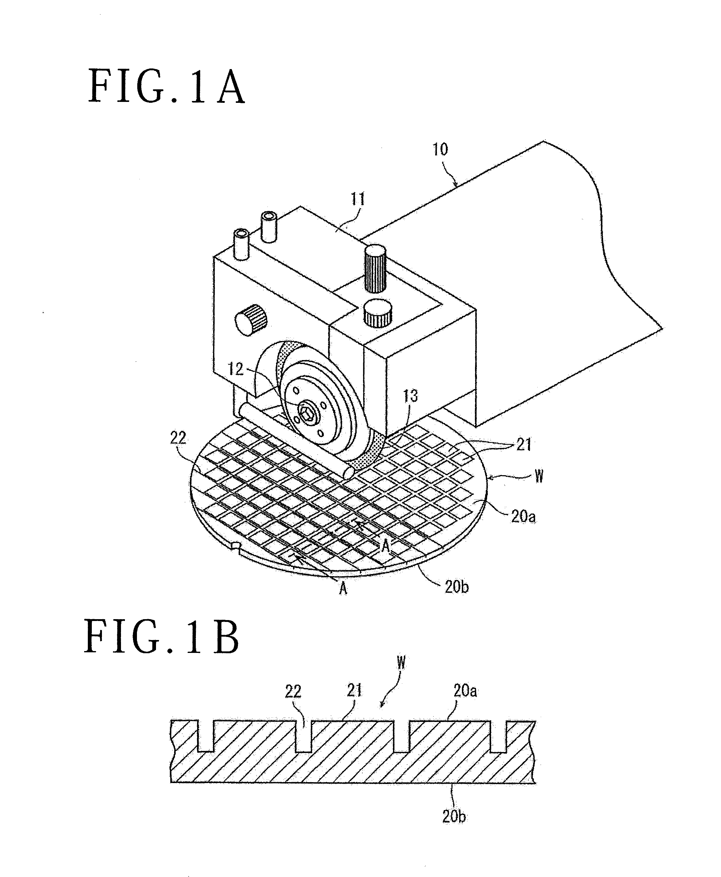
[0028]FIG. 1A depicts the manner in which the step of forming separation grooves is carried out to form separation grooves, each having a depth corresponding to the finished thickness of device chips, in the face side of a semiconductor wafer W along projected division lines formed on the face side of the semiconductor wafer W.

[0029]As depicted in FIG. 1A, the step of forming separation grooves is carried out by a cutting apparatus (omitted in its entirety from illustration), having a spindle unit 10. The spindle unit 10 includes a spindle housing 11 which holds a cutting blade 13 fixedly mounted on the tip end of a spindle 12. The semiconductor wafer W to be steped, which has been fabricated to a predetermined thickness of 700 μm, for example, has a face side 20a that is demarc...


PUM


Abstract

A wafer processing method of processing a wafer with a plurality of devices disposed in areas demarcated by projected division lines and formed on a face side thereof includes a protective member placing step of placing a protective member for protecting the face side of the wafer on the face side of the wafer which is divided into individual device chips, a resin laying step of laying a die-bonding resin on the reverse sides of the individual device chips by applying a die-bonding liquid resin on the reverse side of the wafer and hardening the applied die-bonding liquid resin, and a separation step of separating the device chips with the die-bonding liquid resin laid on the reverse sides thereof from the wafer.

Description

BACKGROUND OF THE INVENTION[0001]Field of the Invention[0002]The present invention relates to a wafer processing method of processing a wafer to form a plurality of device chips with a die-bonding resin provided on the reverse sides thereof.[0003]Description of the Related Art[0004]In the step of fabricating semiconductor devices for use on ICs (Integrated Circuits), LSI (Large Scale Integration) circuits, etc., a wafer with a plurality of devices disposed in areas demarcated by projected division lines and formed on its face side is divided into individual device chips, thereby producing semiconductor device chips. The semiconductor device chips are then packaged for use in electric devices such as mobile phones, personal computers, etc.[0005]The semiconductor device chips are bonded to lead frames (metal boards) or the like. There is known in the art a step of laying a bonding material for bonding the semiconductor device chips to lead frames on the reverse sides of the semiconduc...

Claims


Application Information

Patent Timeline
IPC IPC(8): H01L21/78H01L21/268H01L21/306H01L21/304H01L23/544H01L21/683
CPCH01L21/78H01L23/544H01L21/6835H01L2221/6834H01L21/304H01L21/268H01L2223/54453H01L21/30604H01L21/6836H01L2221/68327H01L2221/68336H01L21/67132H01L21/56H01L21/76H01L21/02013H01L21/67712
Inventor HAIMOTO, TAKASHIKOSHIMIZU, HIDEKIARAYA, YURIKASUGIYA, TETSUKAZU
Owner DISCO CORP
Why Eureka
Try Eureka