Display device
a display device and display technology, applied in the field of display devices, can solve the problems of image quality deterioration, kink phenomenon, deterioration of characteristics of control currents of thin film transistors, etc., and achieve the effect of improving image quality of display devices and suppressing characteristics
- Summary
- Abstract
- Description
- Claims
- Application Information
AI Technical Summary
Benefits of technology
Problems solved by technology
Method used
Image
Examples
first embodiment
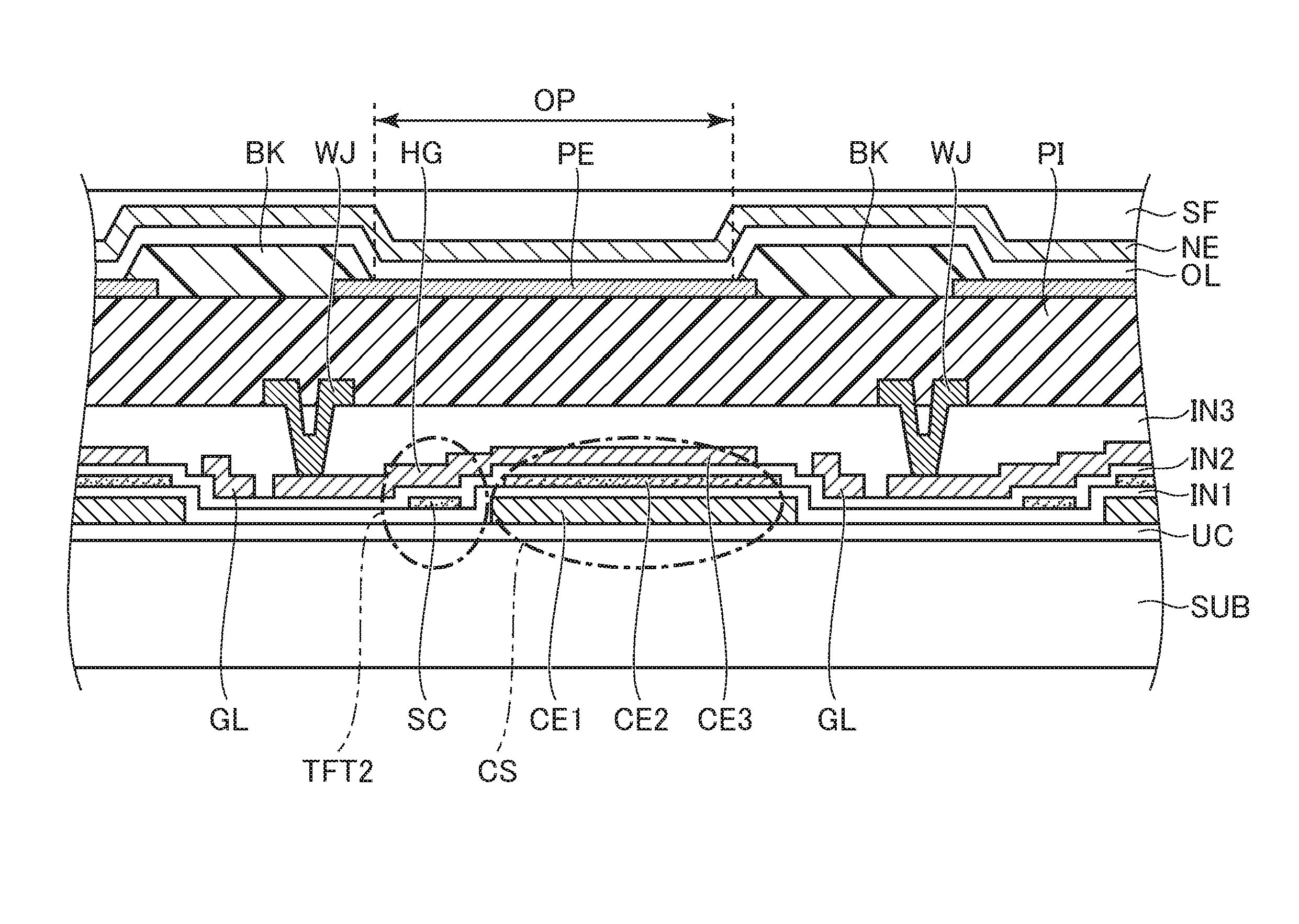
[0033]An organic EL display device according to a first embodiment of the invention includes an array substrate SUB (see FIG. 3), a counter substrate facing the array substrate SUB, a flexible circuit board connected to the array substrate SUB, and a driver integrated circuit. Color filters are provided on the counter substrate, and full-color display is realized by combinations of the color filters and white organic light-emitting diodes (OLEDs). Instead of the white OLEDs, light-emitting elements that emit light of respective colors of RGB or the like may be used, in which case the counter substrate and the color filters may not be present.
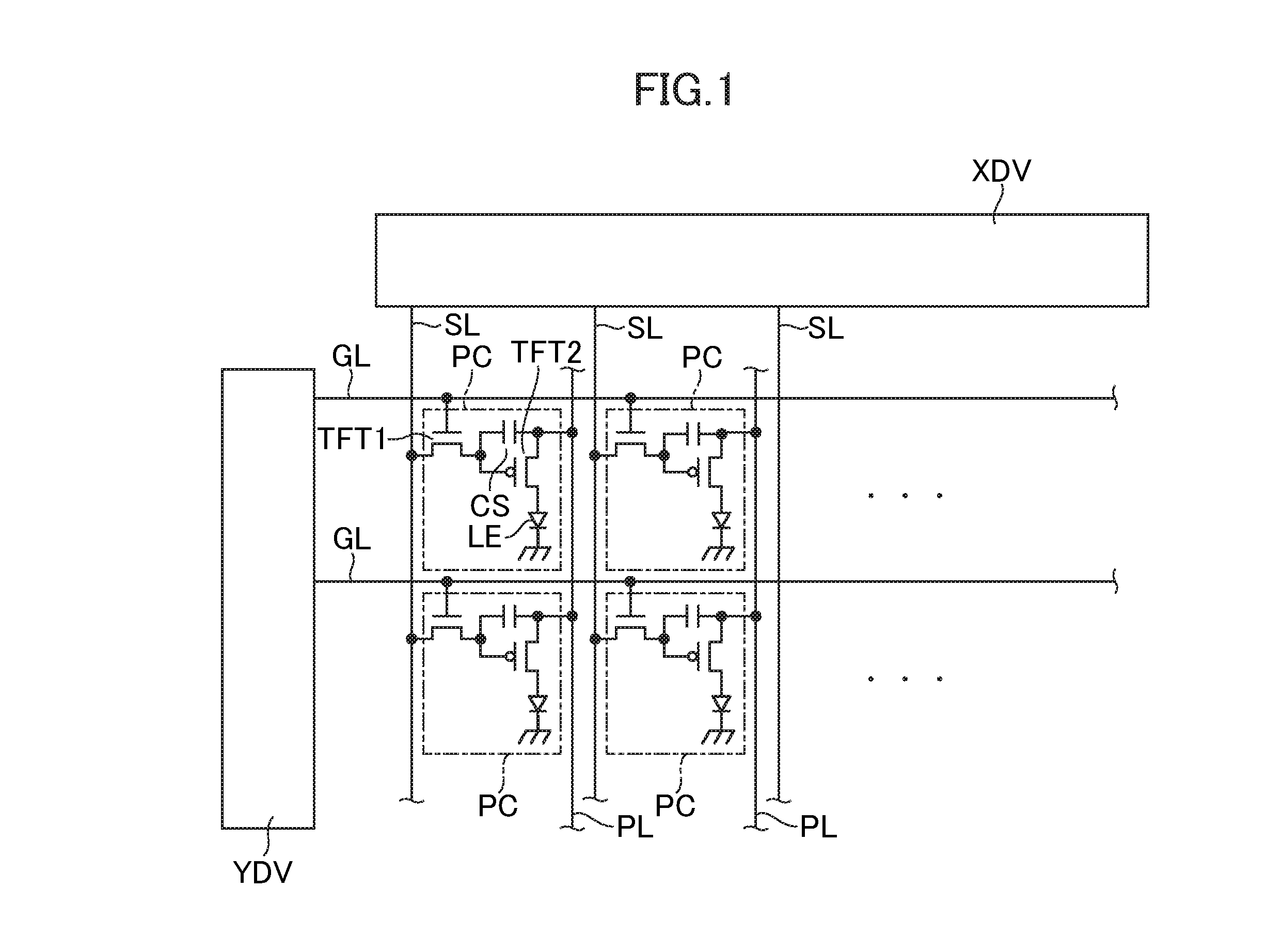
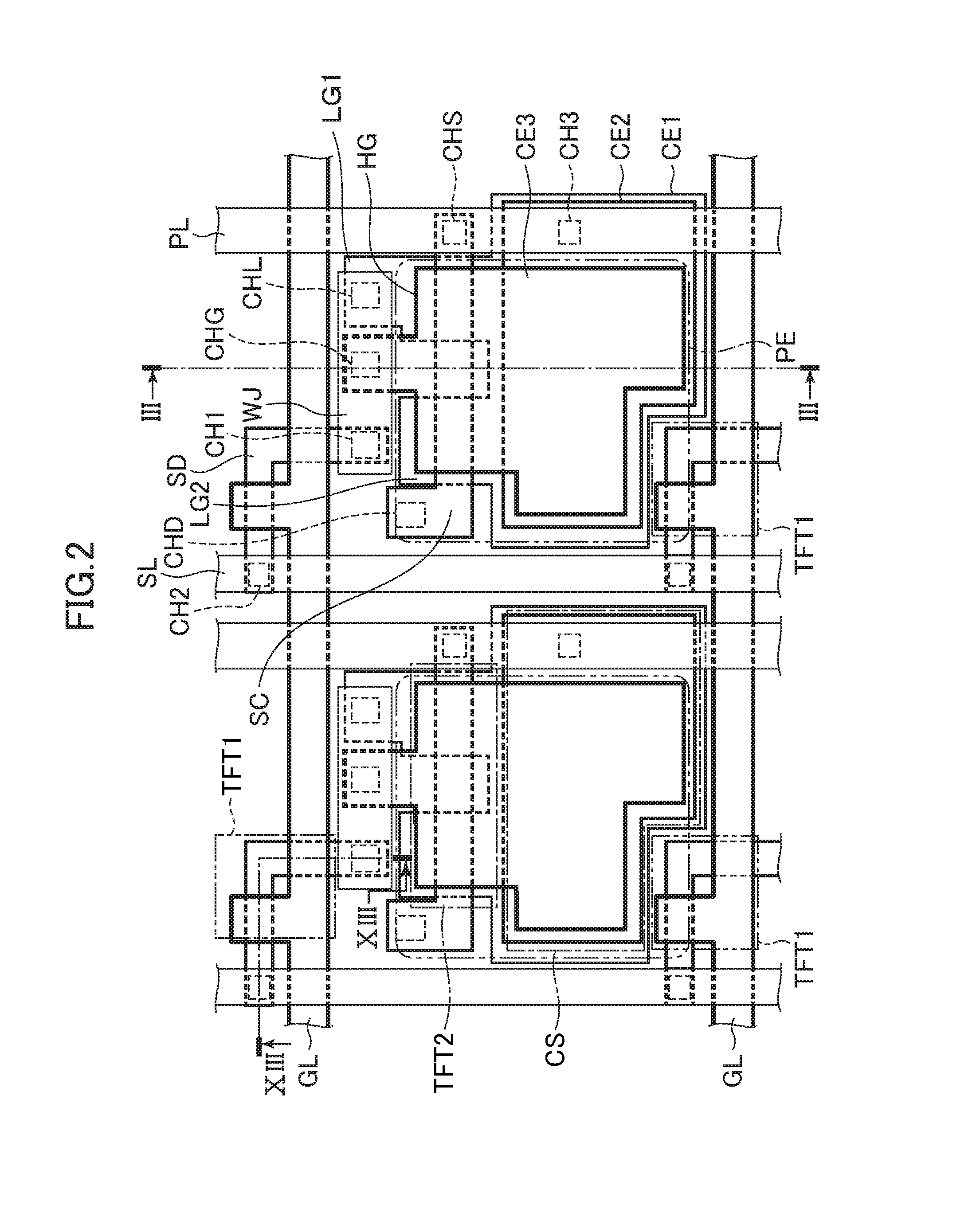
[0034]FIG. 1 is a circuit diagram showing one example of an equivalent circuit of the organic EL display device according to the first embodiment. The circuit shown in FIG. 1 is physically formed on the array substrate SUB (see FIG. 3) or in the driver integrated circuit. A plurality of pixel circuits PC, a plurality of gate signal lines GL, a p...
second embodiment
[0059]Next, an organic EL display device according to a second embodiment of the invention will be described. In the embodiment, a structure for hole accumulation suppression is provided in the channel region. Hereinafter, the organic EL display device according to the second embodiment will be described focusing on different portions from the first embodiment.
[0060]FIG. 10 is a plan view showing one example of the pixel circuit PC according to the second embodiment. Referring to FIG. 10, the channel semiconductor film SC branches off in the upper direction of FIG. 10 in the channel region relative to FIG. 2, and is connected with the power line PL through a contact hole CHH. Moreover, the end of the branched portion of the channel semiconductor film SC is electrically connected with the source region. The lower gate electrodes LG1 and LG2 are provided so as not to overlap the branched portion of the channel semiconductor film SC in a plan view. Moreover, the lower gate electrodes L...
third embodiment
[0065]Next, an organic EL display device according to a third embodiment of the invention will be described. In the embodiment, the channel length is further increased by also using a spacer SP (see FIGS. 14, 15, etc.) formed on the channel semiconductor film SC. Hereinafter, the organic EL display device according to the third embodiment will be described focusing on portions different from the first embodiment, particularly differences in the structure of the thin film transistor TFT2.
[0066]FIG. 14 is a plan view showing one example of the thin film transistor TFT2 according to the third embodiment. FIG. 15 is a cross-sectional view of the thin film transistor TFT2 shown in FIG. 14 along the section line XV-XV.
[0067]The thin film transistor TFT2 shown in FIG. 14 includes the lower gate electrode LG provided on the under layer UC, the channel semiconductor film SC, upper gate electrodes HG1 and HG2, and the spacer SP. The channel semiconductor film SC is provided above the lower ga...
PUM
 Abstract
Description
Claims
Application Information
 - R&D
- Intellectual Property
- Life Sciences
- Materials
- Tech Scout
- Unparalleled Data Quality
- Higher Quality Content
- 60% Fewer Hallucinations
Browse by: Latest US Patents, China's latest patents, Technical Efficacy Thesaurus, Application Domain, Technology Topic, Popular Technical Reports.
© 2025 PatSnap. All rights reserved.Legal|Privacy policy|Modern Slavery Act Transparency Statement|Sitemap|About US| Contact US: help@patsnap.com


