
Method for manufacturing semiconductor device

a manufacturing method and technology of semiconductor devices, applied in the direction of semiconductor devices, electrical devices, transistors, etc., can solve the problems of line edge roughness and gate length fluctuation in one gate electrode, and achieve the effect of suppressing the fluctuation in characteristics of the particular device and high accuracy

Inactive Publication Date: 2007-03-01
RENESAS ELECTRONICS CORP
View PDF10 Cites 0 Cited by
  • Summary
  • Abstract
  • Description
  • Claims
  • Application Information

AI Technical Summary

Benefits of technology

[0010] According to another aspect of the present invention, there is provided a method of manufacturing a semiconductor device that includes performing a first etching process on a wiring layer to form a passive device formed by wiring layer, and performing a second etching process different from the first etch to form a line having a specified shape. Forming in this way enables a passive device to be highly accurate.
[0011] Providing a process to form only a particular device, it is possible to greatly suppress a fluctuation in characteristics of the particular device to.

Problems solved by technology

Furthermore in MISFET for example, besides a fluctuation in gate length (electrode width) between devices, a fluctuation of gate length in one gate electrode (LER: Line Edge Roughness) has become problematic.

Method used


Image

  • Method for manufacturing semiconductor device
  • Method for manufacturing semiconductor device
  • Method for manufacturing semiconductor device

Examples


second embodiment

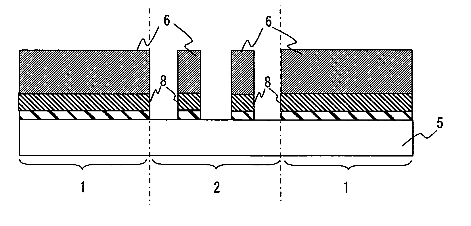
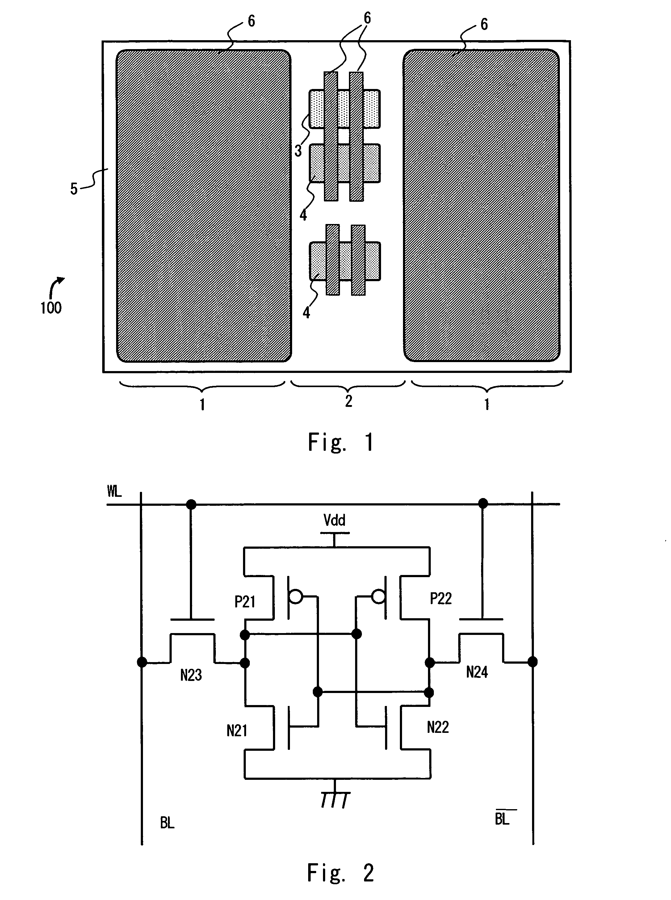
[0035]FIG. 7 is a view explaining a method of manufacturing a semiconductor device 200 of a second embodiment. In a semiconductor device of recent years, a passive device (capacitance, inductance, and resistance) is formed using a conductive layer such as a metal wiring. FIG. 7 is a pattern diagram showing a case of forming an inductance (coil) 81 using a conductive layer. The conductive layer forming the inductance 81 in this example is used as a wiring in other region of a semiconductor device. As described in the foregoing, the semiconductor device 200 of the second embodiment includes a passive device forming region 82 by metal wiring layer, and a normal metal wiring forming region 83. The metal wiring layer of the normal metal wiring forming region 83 only needs to be formed for satisfying design standard about a delay and resistance of wiring. On the other hand, to form a passive device by the same conductive layer as the metal wiring, a highly accurate processing is required ...


PUM


Abstract

A method of manufacturing a semiconductor device includes performing a first etching process on a gate electrode layer to form a gate electrode of a first transistor group including a transistor pair, and performing a second etching process different from the first etching on the gate electrode layer to form a gate electrode of a second transistor group. Forming in this way enables characteristics of the transistor pair to be the same.

Description

BACKGROUND OF THE INVENTION [0001] 1. Field of the Invention [0002] The present invention relates to a manufacturing method of a semiconductor device, and particularly to a method of manufacturing a plurality of devices having the same characteristics or a highly accurate device. [0003] 2. Description of Related Art [0004] Conventionally in a semiconductor integrated circuit device, a multitude of pair field effect transistors (hereinafter referred to as MISFET) are used in a circuit. The pair MISFETs are used in a flip-flop circuit, a sense amplifier circuit in a memory storage, and a memory cell of a Static Random Access Memory (hereinafter referred to as SRAM), for example. Further, a difference in characteristics of those transistor pairs influence yield factor, performance and fluctuation in characteristics of an integrated circuit. In a semiconductor device where transistors are supposed to have the same characteristics, it is known that production tolerance produces a fluctua...

Claims


Application Information

Patent Timeline
Patent Type & Authority Applications(United States)
IPC IPC(8): H01L21/8238
CPCH01L21/32139H01L27/1104H01L27/11H01L21/823456H10B10/00H10B10/12
Inventor NAGATA, TAKAMIFURUTA, HIROSHI
Owner RENESAS ELECTRONICS CORP
Learn More