Conductive barrier direct hybrid bonding

a technology of conductive barrier and hybrid bonding, which is applied in the direction of semiconductor/solid-state device details, electrical equipment, semiconductor devices, etc., can solve the problem of typical heterogeneous bonding between metal on one surface and dielectric on the other surfa

Active Publication Date: 2017-03-02
INVENSAS BONDING TECH INC
View PDF4 Cites 156 Cited by
  • Summary
  • Abstract
  • Description
  • Claims
  • Application Information

AI Technical Summary

Problems solved by technology

However, when these surfaces are used for hybrid bonding, there will typically be a heterogeneous bond component between metal on one surface and dielectric on the other surface, for example due to misalignment of via surfaces.
It has been relatively more challenging to leverage an Al BEOL industry standard process because the two primary metals in this process, W and Al, are more challenging materials to develop either a W or Al direct hybrid bond technology due to a combination of factors including high yield strength, coefficient of thermal expansion (CTE), native oxide, and hillock formation.

Method used


Image

  • Conductive barrier direct hybrid bonding
  • Conductive barrier direct hybrid bonding
  • Conductive barrier direct hybrid bonding

Examples


Embodiment Construction

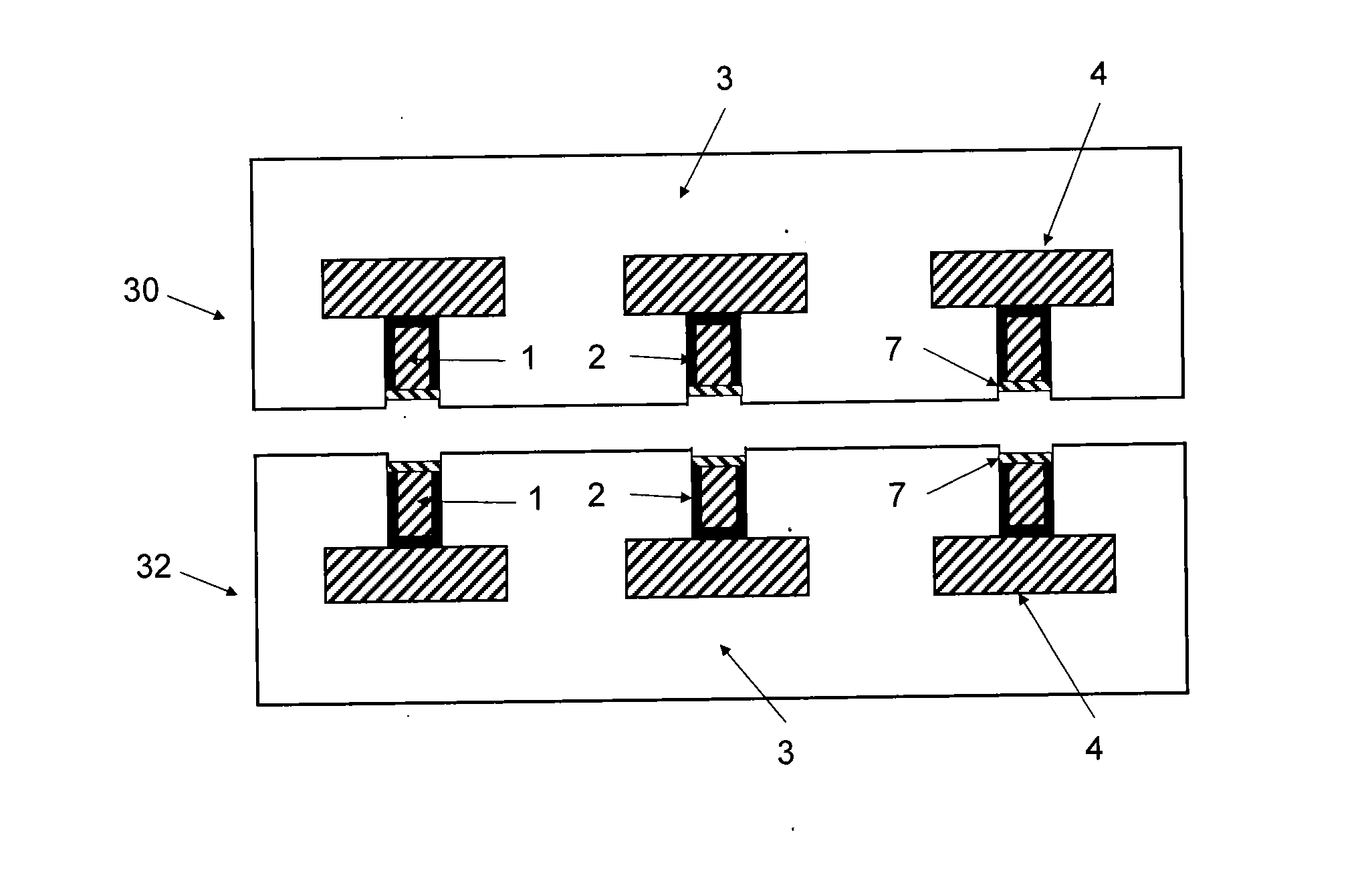
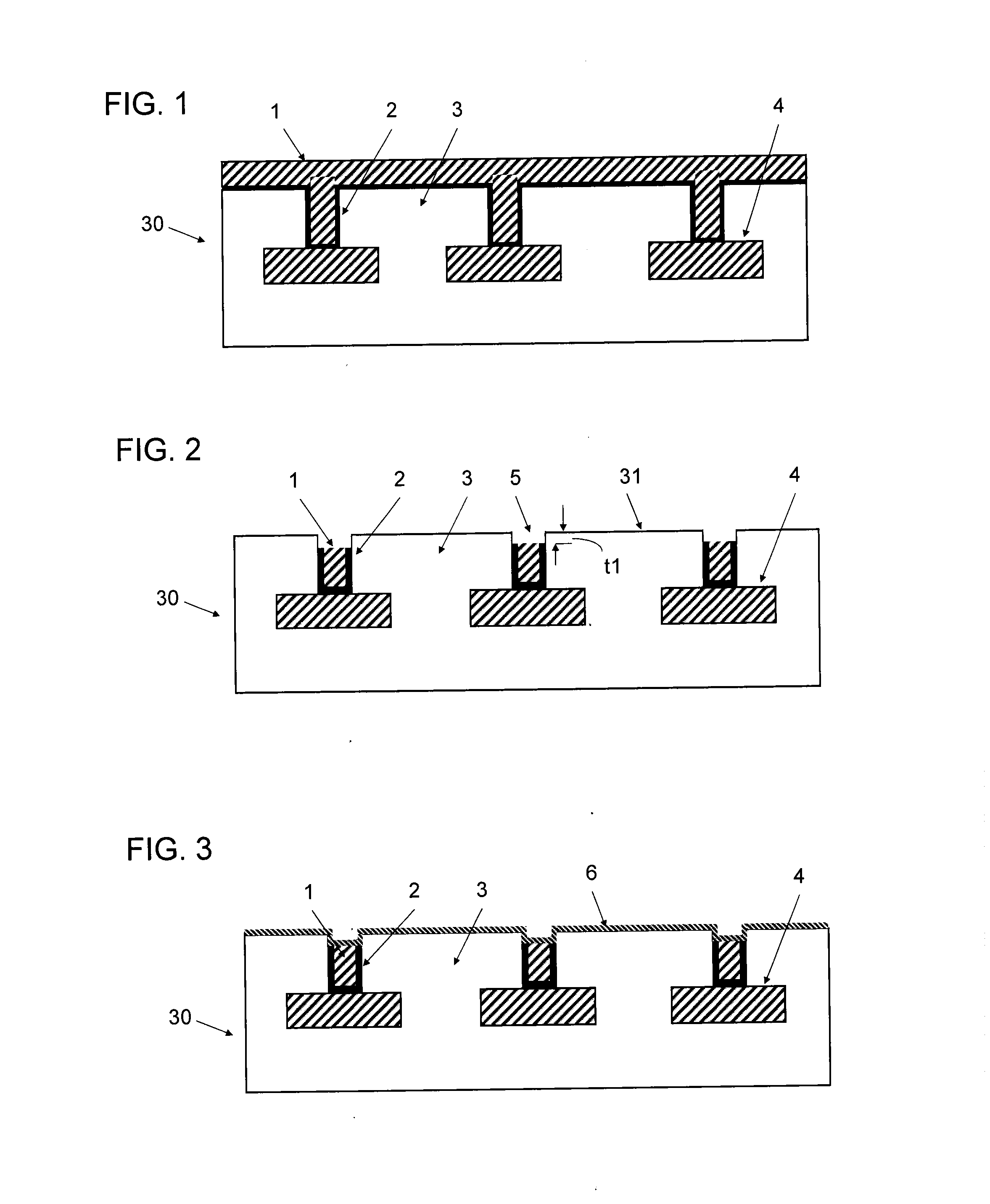
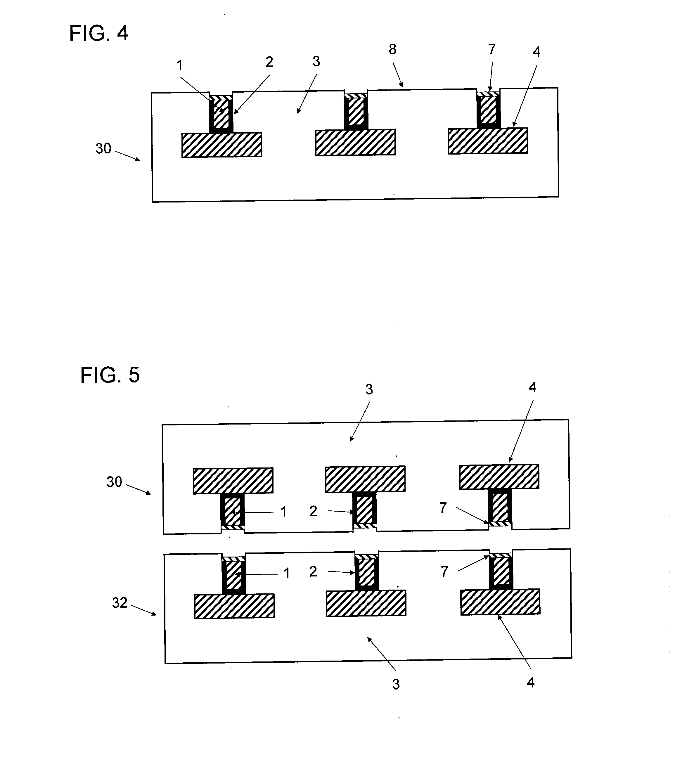
[0027]Referring now to the drawings, wherein like reference numerals designate like or corresponding parts throughout the several views, and more particularly to FIG. 1 showing a cross-section of a surface of a substrate 30 in a process for direct hybrid bonding according to the invention comprised of conductor 1, conductive barrier 2, dielectric 3, and metal structure 4. Metal structures 4 are formed in dielectric 3. Metal structures 4 are located within dielectric 3 and can be a contact, pad, line, or other metal interconnect structure. Openings are formed in dielectric 3 over metal structures 4 followed by formation of barrier 2 and conductor 1. The sizes and thicknesses of the conductor 1, conductive barrier 2 and metal structure 4 are not to scale but are drawn to illustrate the invention. While the openings and metal structures are shown to be the same size and shape, they can differ in size and shape depending upon design or need.

[0028]A wide variety of metals for conductor 1...


PUM

PropertyMeasurementUnit
roughnessaaaaaaaaaa
temperaturesaaaaaaaaaa
temperatureaaaaaaaaaa

Abstract

A method for forming a direct hybrid bond and a device resulting from a direct hybrid bond including a first substrate having a first set of metallic bonding pads, preferably connected to a device or circuit, capped by a conductive barrier, and having a first non-metallic region adjacent to the metallic bonding pads on the first substrate, a second substrate having a second set of metallic bonding pads capped by a second conductive barrier, aligned with the first set of metallic bonding pads, preferably connected to a device or circuit, and having a second non-metallic region adjacent to the metallic bonding pads on the second substrate, and a contact-bonded interface between the first and second set of metallic bonding pads capped by conductive barriers formed by contact bonding of the first non-metallic region to the second non-metallic region.

Description

CROSS-REFERENCE TO RELATED APPLICATIONS[0001]This application is related to application Ser. Nos. 09 / 505,283, 10 / 359,608 and 11 / 201,321, the entire contents of which are incorporated herein by reference.BACKGROUND OF THE INVENTION[0002]Field of the Invention[0003]The present invention relates to the field of direct bonding, more specifically hybrid direct bonding, preferably at room or low temperature, and more particularly to the bonding of semiconductor materials, devices, or circuits to be utilized in stacked semiconductor device and integrated circuit fabrication and even more particularly to the fabrication of value-added parts in consumer and business products including image sensors in mobile phones, RF front ends in cell phones, 3D memory in high performance graphics products, and 3D memory in servers.[0004]Description of the Related Art[0005]Die, chip, or wafer stacking has become an industry standard practice to the continuing demands of increased functionality in a smalle...

Claims


Application Information

Patent Timeline
Patent Type & Authority Applications(United States)
IPC IPC(8): H01L23/00H01L25/065H01L25/00
CPCH01L24/09H01L24/03H01L24/89H01L25/50H01L25/0657H01L2224/08145H01L2224/05082H01L2224/05005H01L2224/05078H01L2224/8019H01L2224/80895H01L2224/036H01L24/08H01L24/80H01L21/50H01L21/52H01L24/04H01L24/05H01L21/2007H01L21/187H01L24/28H01L24/27H01L2224/08121H01L2224/80194H01L2224/80031H01L2224/80075H01L2225/06513H01L2224/03825H01L2224/05007H01L2224/05686H01L2224/05124H01L2224/0345H01L2224/80035H01L2224/05681H01L2224/08112H01L2224/05684H01L2224/03462H01L2224/03616H01L2224/03452H01L2224/05562H01L2224/05561H01L2224/05676H01L2224/08147H01L2224/80986H01L2224/80099H01L2224/80011H01L2224/0603H01L2224/80097H01L2224/80935H01L2224/05547H01L2224/80896H01L2224/05026H01L2224/05147H01L2224/05666H01L2224/08137H01L2224/05657H01L2224/05655H01L2224/8034H01L2224/80047H01L2224/05571H01L2224/08123H01L2224/05573H01L2924/00014H01L2224/29339H01L2224/29386H01L2924/053H01L2924/04941H01L2924/04953H01L2924/049H01L2924/01014H01L2924/01005H01L2924/01074H01L2924/051H01L2924/042H01L24/26H01L24/83H01L2224/27H01L2224/30505H01L2224/29287H01L2224/293H01L2224/3001H01L2224/3005H01L2224/8303H01L2224/83203
Inventor ENQUIST, PAUL M.
Owner INVENSAS BONDING TECH INC
Why Eureka
Try Eureka