LED package structure with an integrated pin to transmit operation power and control signals

Active Publication Date: 2017-03-02
HUANG HSIEN JUNG
View PDF3 Cites 1 Cited by
  • Summary
  • Abstract
  • Description
  • Claims
  • Application Information

AI Technical Summary

Benefits of technology

The LED package structure in this invention has a reduced number of PIN (P-type layer, Intrinsic layer, and N-type layer) to achieve mass production at low cost.

Problems solved by technology

Due to plenty of nonstop technology advancements, the conventional single-color LED is gradually unable to satisfy human's visual needs.
Therefore, in the limited space of the full-color LED, it is difficult to achieve mass production with low costs and high production yield rate.

Method used


Image

  • LED package structure with an integrated pin to transmit operation power and control signals
  • LED package structure with an integrated pin to transmit operation power and control signals
  • LED package structure with an integrated pin to transmit operation power and control signals

Examples


first embodiment

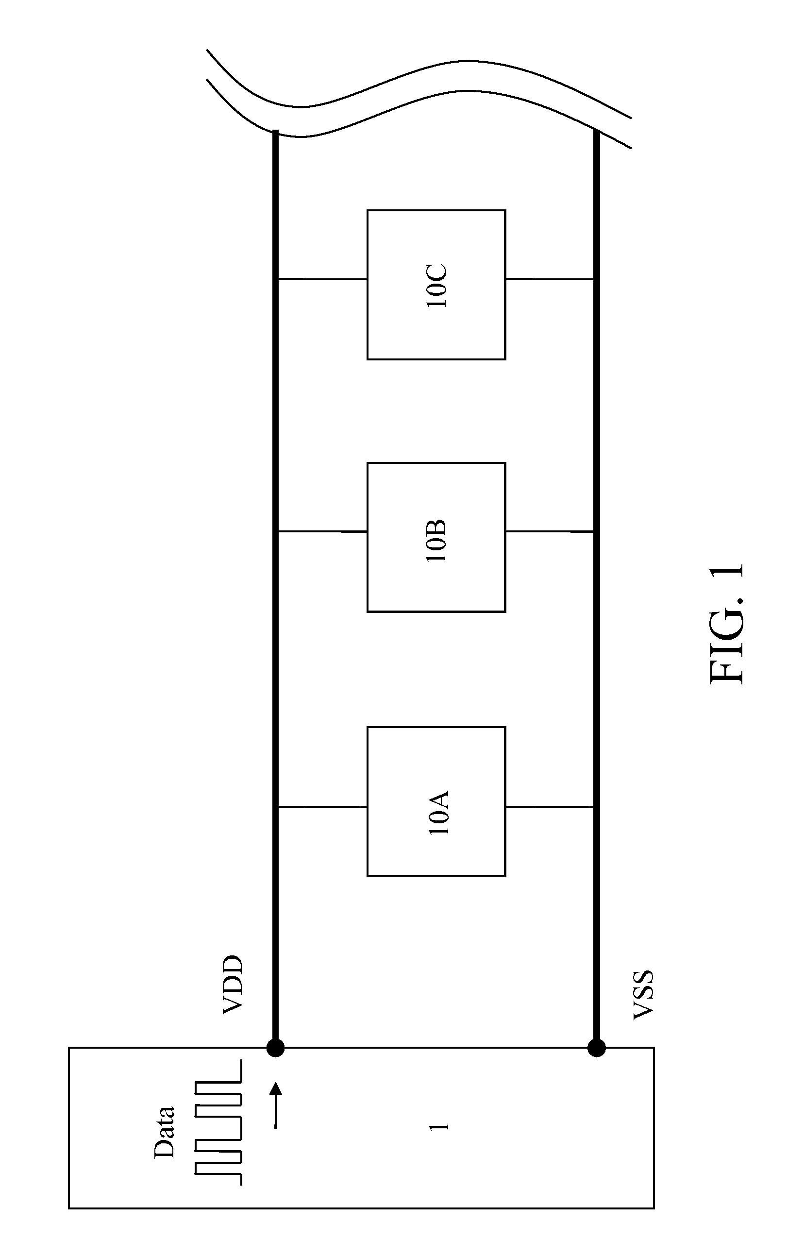
[0027]Please refer to FIG. 1, which is a schematic view of an LED display system according to the present invention.

[0028]The LED display system of this invention includes a main control 1 and a plurality of LED (Light Emitting Diode) 10A, 10B, and 10C, which connected in parallel. The main control 1 is used to generate an operation power and a PWM (Pulse Width Modulation) signal Data to the LEDs 10A, 10B, and 10C. As shown in FIG. 1, the main control 1 may only include a power input pin VDD and a ground pin VSS to control the LEDs 10A, 10B, and 10C. The operation power and the PWM signal Data are transmitted from the power input pin VDD.

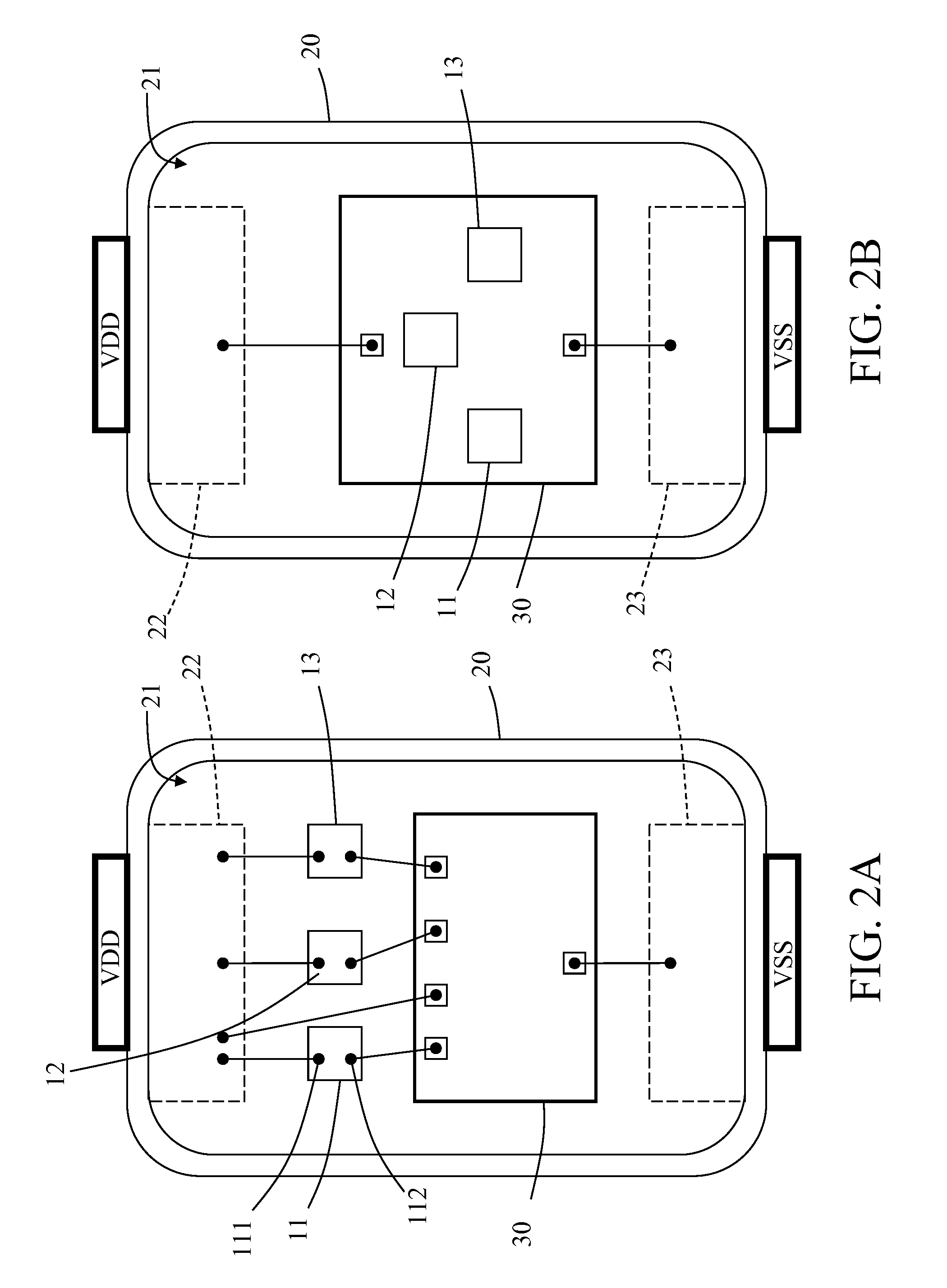
[0029]FIG. 2A is a schematic view of a first embodiment of an LED package structure according to the present invention.

[0030]The LED package structure in the present invention includes a carrier 20, at least one group of pins, and a driver element 30. The carrier 20 has an inner space 21 to dispose a red LED dice 11, a green LED dice 12 and a blue L...

second embodiment

[0033]FIG. 3A is a schematic view of an LED package structure according to the present invention.

[0034]The LED package structure includes a power input pin VDD and a ground pin VSS. The driver element 30 is pasted on the frame-type extension portion 23 of the ground pin VSS. And the red, green and blue LED dices 11, 12, and 13 are pasted on the frame-type extension portion 22 of the power input pin VDD. The light-mixing glue of light-pervious material is feed to complete the bulb-type package.

[0035]FIG. 3B is a schematic view of another example of the second embodiment of an LED package structure according to the present invention. In this embodiment, the red, green and blue LED dices 11, 12, and 13 are pasted on the driver element 30 directly to form electrical connections with the driver element. Therefore, the amount of bonding wires is reduced.

[0036]Please refer to FIG. 4, which is a schematic view of a second embodiment of an LED display system according to the present inventio...

third embodiment

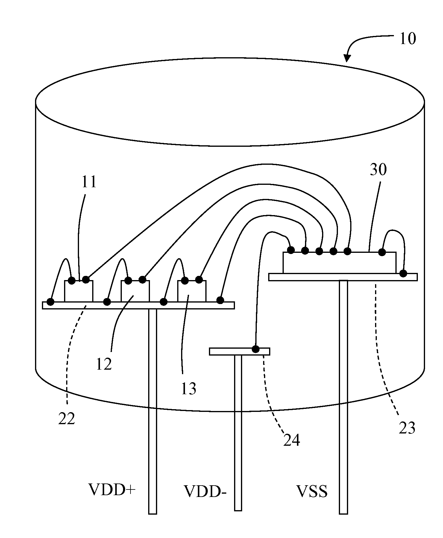
[0038]FIG. 5A is a schematic view of an LED package structure according to the present invention.

[0039]Each group of pins includes a power input pin VDD+, a power output pin VDD− and a ground pin VSS. And each of the power input pin VDD+, the power output pin VDD− and the ground pin VSS has an extension portion 22, 23, and 24 extended inside of the carrier 20. The first electrode 111 of each of the red, green and blue LED dices 11, 12, and 13 is connected to the extension portion 22 of the power input pin VDD+. The driver element 30 is pasted inside the carrier 20 and respectively connected with the second electrode 112 of each of the red, green and blue LED dices 11, 12, and 13 by using bonding wires. And the driver element 30 is connected to the extension portions 22, 23, and 24 of the power input pin VDD+, the power output pin VDD− and the ground pin VSS. Then, the light-mixing glue of light-pervious material is feed to complete the package. The driver element 30 may control the ...


PUM


Abstract

A LED package structure is provided. The LED package includes a three-element red-green-blue (RGB) light emitting diode (LED). The carrier of the LED package has a power input pin and a ground pin and the pins form extension portions inside the carrier. The driver element, a red dice, a green dice, and a blue dice are disposed within the carrier. The driver element controls the red, green and blue LED dices by receiving an operation power and a PWM (Pulse Width Modulation) signal from the power input pin. By this arrangement, the LED package with compact structure, good mixing effect, and high resolution is achieved. Furthermore, the using space is saved and the PIN number is reduced to allow mass production with low costs.

Description

BACKGROUND OF THE INVENTION[0001]Field of the Invention[0002]The present invention relates to a package structure of full-color LED (Light Emitting Diode) adapted to various LED display systems with saved using space, and more particularly, to a package structure of LED with an integrated pin to transmit operation power and control signals.[0003]Related Art[0004]Light plays a significant role for a very long time in human life. Accompanying with the constant progresses of science and technology, LED (Light Emitting Diode) has been invented in 1970s. With the advantages of compact size, long lifetime, low breakage, low power consumption, no heat radiation and no toxic pollution (such as mercury and etc.), comparing with conventional light sources, LED is now broadly utilized in our daily life.[0005]Through the environment / economization policies driven by the governments around the world, LED is well-developed and applied to two major applications including display and illumination fu...

Claims


Application Information

Patent Timeline
IPC IPC(8): H05B33/08H05B33/06H05B44/00
CPCH05B33/0821H05B33/0842H05B33/06H01L2224/48091H01L2924/181H01L2224/48137H01L2224/48247H01L2224/48257H05B45/00H05B45/20H05B45/325H01L2924/00014H01L2924/00012
Inventor HUANG, HSIEN-JUNG
Owner HUANG HSIEN JUNG
Why Eureka
Try Eureka