Eureka AIR delivers breakthrough ideas for toughest innovation challenges, trusted by R&D personnel around the world.

Image processing chip and related method thereof

Active Publication Date: 2007-09-13
REALTEK SEMICON CORP
View PDF22 Cites 0 Cited by
  • Summary
  • Abstract
  • Description
  • Claims
  • Application Information

AI Technical Summary

Benefits of technology

[0007]It is therefore one of the objectives of the claimed invention to provide an image processing chip and related method for reducing the number of the pins required to achieve said task.

Problems solved by technology

The above-mentioned method of utilizing two pins to receive the same composite signal is quite uneconomical.
Therefore, the chip size and the cost to manufacture the chip will significantly increase.

Method used


Image

  • Image processing chip and related method thereof
  • Image processing chip and related method thereof
  • Image processing chip and related method thereof

Examples


Embodiment Construction

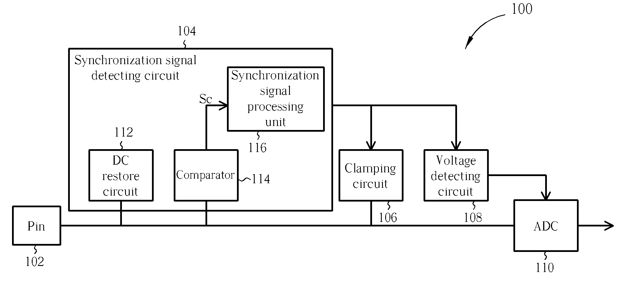
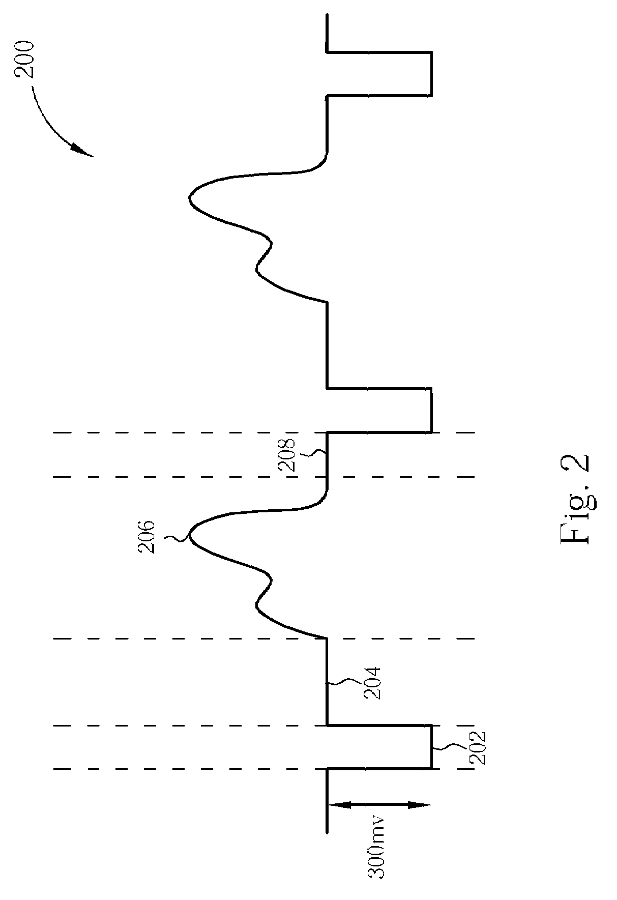
[0014]Please refer to FIG. 2. FIG. 2 is a schematic diagram of a composite signal 200 received by the image processing chip of the present invention. The composite signal 200 mentioned in the following text is the above-mentioned SOG signal, SOY signal, or any other video signal attached to the synchronization signal described in the prior art. As shown in the FIG. 2, the composite signal 200 is approximately divided into several blocks 202, 204, 206, and 208. The block 202 attaches the synchronization signal; the block 206 attaches the video signal; and blocks 204 and 208 provide the black level of the video signal. When the image processing chip processes the video signal of the block 206, the image processing chip needs a reference voltage level for correctly detecting the content of the video image. Therefore, the blocks 204 and 208 then provide the reference voltage level. Generally speaking, the voltage difference between the blocks 202 and 204 is 300 mV. However, the above-me...


PUM


Abstract

The invention relates to an image processing chip and related method. The image processing chip includes a pin for receiving a composite signal; a synchronization signal detecting circuit, coupled to the pin, for extracting a synchronization signal from the composite signal; a clamping circuit, coupled to the pin, for adjusting a voltage level of the composite signal according to the synchronization signal; and an analog to digital converter, coupled to the pin, for generating a video signal by sampling the composite signal.

Description

BACKGROUND OF THE INVENTION [0001]1. Field of the Invention[0002]The invention relates to an image processing chip and related method thereof, and more particularly, to an image processing chip capable of separating video signals and synchronization signals and the related method thereof.[0003]2. Description of the Prior Art[0004]Generally, a monitor can process and display a received video signal according to a horizontal synchronization signal and a vertical synchronization signal. In certain transmission interfaces with specific standards, the horizontal synchronization signal and the vertical synchronization signal are firstly integrated into a composite sync signal, and the composite sync signal is then attached to an image signal. For instant, a G signal of the RGB signal is associated with a green color, or the Y signal of the YPbPr signal is associated with a luminance. The above-mentioned green signal with the synchronization signal is also referred to as the SOG signal (i....

Claims


Application Information

Patent Timeline
IPC IPC(8): H03M1/12H04N5/16
CPCH04N5/185H04N5/08
Inventor GONG, JIN-SHENGTSAI, JUI-YUANCHOU, YU-PINHUANG, YUEH-HSING
Owner REALTEK SEMICON CORP
Why Eureka
Eureka Blog
Learn More