
OLED Display Panel And Manufacturing Method Thereof

a technology of oled display panel and manufacturing method, which is applied in the direction of basic electric elements, electrical apparatus, semiconductor devices, etc., can solve the problems of oled display screen display effect and display effect also being affected, and achieve the effect of improving the accuracy of emitted color of oled panel

Active Publication Date: 2017-03-16
EVERDISPLAY OPTRONICS (SHANGHAI) CO LTD
View PDF2 Cites 3 Cited by
  • Summary
  • Abstract
  • Description
  • Claims
  • Application Information

AI Technical Summary

Benefits of technology

The patent text describes a new method for manufacturing OLED display panels that solves the issue of color shifting at low gray levels. The method involves adding a layer between the anode and OLED device layer or between the OLED device layer and cathode, which adjusts the thickness or doping concentration of the layer to improve the accuracy of emitting color. This results in a more accurate and reliable display.

Problems solved by technology

As a display device, the OLED display screen may also be affected by environmental factors; especially in a strong light environment, the display effect of the OLED display screen will also decline.

Method used


Image

  • OLED Display Panel And Manufacturing Method Thereof
  • OLED Display Panel And Manufacturing Method Thereof
  • OLED Display Panel And Manufacturing Method Thereof

Examples


embodiment 1

[0061]To solve the color shift problem under low gray-scale caused by different cut-in voltage of sub-pixels of the OLED in the prior art, the present disclosure provides an OLED display panel which has a low gray color shift adjustment layer, and solves the color shift problem under low gray-scale through adjusting thickness or doping concentration of the low gray color shift adjustment layer, and improves the accuracy of emitting color of the OLED panel.

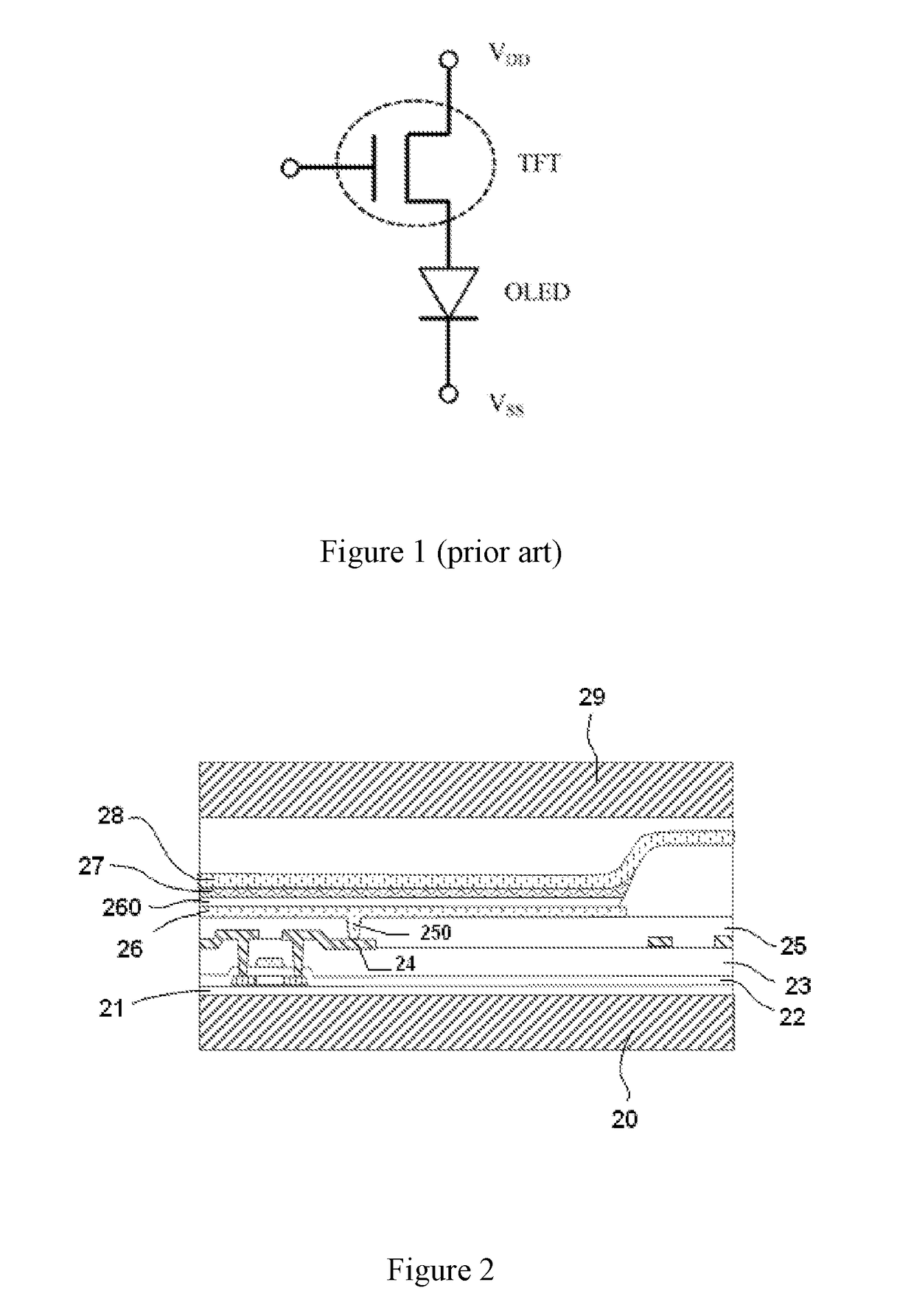
[0062]Specifically, a structure as shown in the FIG. 2, the OLED display panel mainly comprises:[0063]a substrate 20; and a buffer layer 21, a gate insulating layer 22 and an insulating layer 23 covering on the substrate 20 in order;[0064]a thin-film transistor 24 configured on the substrate 20; and part of the thin-film transistor 24 is positioned between the gate insulating layer 22 and the insulating layer 23;[0065]a planarizing layer 25 configured on the thin-film transistor 24; and part of the thin-film transistor 24 is positi...

embodiment 2

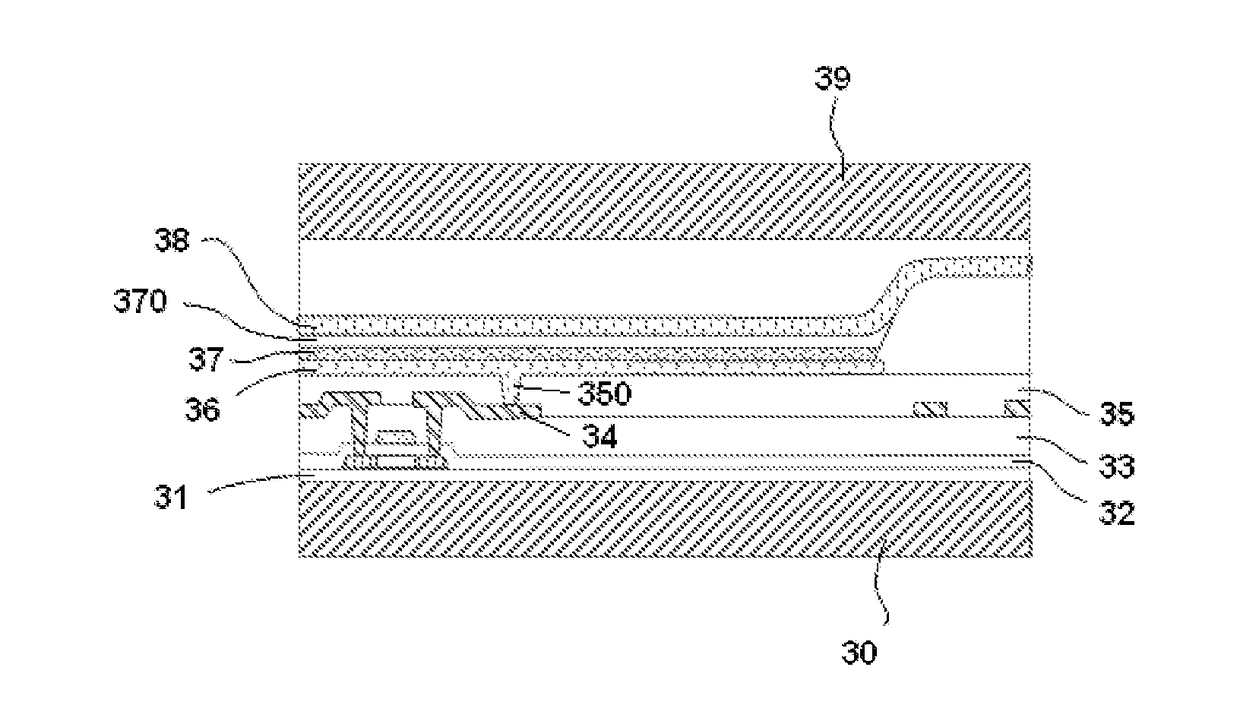
[0082]In the embodiments of the disclosure, the technical solution recorded in Embodiment 1 is also applicable for Embodiment 2, so the technical solution of Embodiment 1 will not be repeat here, the obvious differences between Embodiment 2 and Embodiment 1 are: the OLED display panel mainly comprises (as shown in FIG. 3):[0083]a substrate 30; and a buffer layer 31, a gate insulating layer 32 and an insulating layer 33 covering on the substrate 30 in order;[0084]a thin-film transistor 34 configured on the substrate 30, and part of the thin-film transistor 34 is positioned between the gate insulating layer 32 and the insulating layer 33;[0085]a planarizing layer 35 configured on the thin-film transistor 34, and part of the thin-film transistor 34 is positioned in the planarizing layer 35; and the planarizing layer 35 comprises a through-hole 350 penetrating the planarizing layer 35 to the thin-film transistor 34;[0086]a first electrode 36 configured on the planarizing layer 35, and e...

embodiment 3

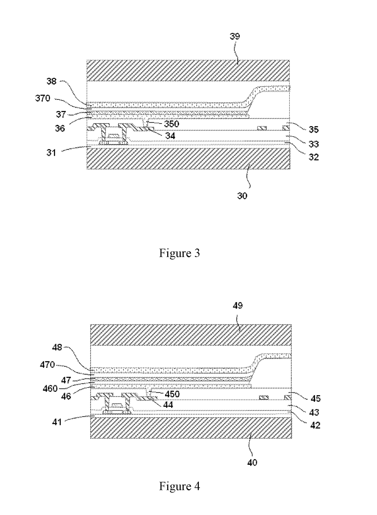
[0093]In the embodiments of the disclosure, the technical solution recorded in Embodiment 1 is also applicable for Embodiment 3, so it will not be repeat here, the obvious differences between Embodiment 3 and Embodiment 1 are: the OLED display panel mainly comprises (as shown in FIG. 4):[0094]a substrate 40; and a buffer layer 41, a gate insulating layer 42 and an insulating layer 43 covering on the substrate 40 in order;[0095]a thin-film transistor 44 configured on the substrate 40, and part of the thin-film transistor 44 is positioned between the gate insulating layer 42 and the insulating layer 43;[0096]a planarizing layer 45 configured on the thin-film transistor 44, and part of the thin-film transistor 44 is positioned in the planarizing layer 45; and the planarizing layer 45 comprises a through-hole 450 penetrating the planarizing layer 45 to the thin-film transistor 44;[0097]a first electrode 46 configured on the planarizing layer 45, and electrically connected to the thin-fi...


PUM


Abstract

The disclosure relates to the field of OLED display technology, more particularly, to an OLED display panel and a manufacturing method thereof, during the manufacturing process of the OLED display panel, by forming a low gray color shift adjustment layer between the anode and the OLED device layer, and / or between the OLED device layer and the cathode, so as to solve the color shift problem under low gray-scale by adjusting thickness or doping concentration of the low gray color shift adjustment layer, and improve the accuracy of emitting color of the OLED panel.

Description

CROSS-REFERENCE TO RELATED APPLICATIONS[0001]The present application claims priority to and the benefit of Chinese Patent Application No. CN 201510582959.5, filed on Sep. 14, 2015, the entire content of which is incorporated herein by reference.BACKGROUND OF THE DISCLOSURE[0002]Field of the Disclosure[0003]The disclosure relates to the field of OLED display technology, more particularly, to an OLED display panel and a manufacturing method thereof.[0004]Description of the Related Art[0005]OLED (organic light-emitting diode) has been widely used in digital products due to its features like lightweight and power saving. OLED display technology is different compared with the traditional LCD (liquid crystal display) display mode; OLED display technology needs no backlight and uses very thin organic material coating and glass substrate; the organic materials will shine when electric current passes through. As a display device, the OLED display screen may also be affected by environmental ...

Claims


Application Information

Patent Timeline
Patent Type & Authority Applications(United States)
IPC IPC(8): H01L27/32H01L51/56H01L51/52
CPCH01L27/3258H01L27/3262H01L51/56H01L51/5218H01L51/5234H01L51/5237H10K50/155H10K50/165
Inventor MOU, XINTSOU, CHUNG CHELIN, HSIN CHIHZHANG, BIN
Owner EVERDISPLAY OPTRONICS (SHANGHAI) CO LTD
Learn More