Monolithic ceramic capacitor

a ceramic capacitor and monolithic technology, applied in the direction of stacked capacitors, fixed capacitor details, fixed capacitor terminals, etc., can solve the problems of reducing the yield of a manufacturing process, reducing the reliability of the product, and reducing the likelihood of delamination, so as to reduce or prevent the occurrence of delamination

Active Publication Date: 2017-03-30
MURATA MFG CO LTD
View PDF10 Cites 3 Cited by
  • Summary
  • Abstract
  • Description
  • Claims
  • Application Information

AI Technical Summary

Benefits of technology

[0010]Accordingly, preferred embodiments of the present invention address the above-described problems and provide a large-capacity monolithic ceramic capacitor in which the occurrence of delamination is significantly reduced or prevented.
[0019]With various preferred embodiments of the present invention, large-capacity monolithic ceramic capacitors that significantly reduces or prevents the occurrence of delamination are provided.

Problems solved by technology

However, when the continuity of the conductor layers is increased, delamination is likely to occur.
The delamination may cause a decrease in reliability of the product and a decrease in yield in a manufacturing process.

Method used


Image

  • Monolithic ceramic capacitor
  • Monolithic ceramic capacitor
  • Monolithic ceramic capacitor

Examples


first preferred embodiment

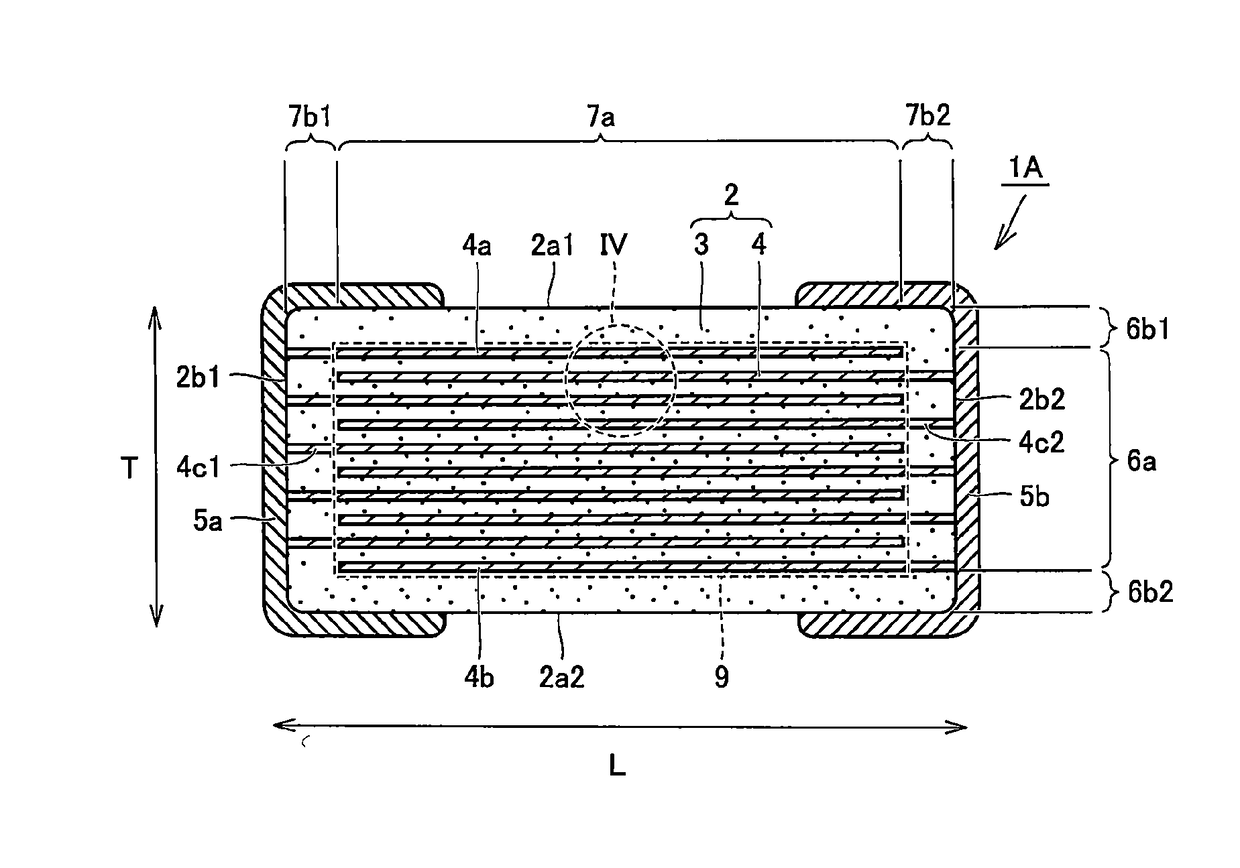
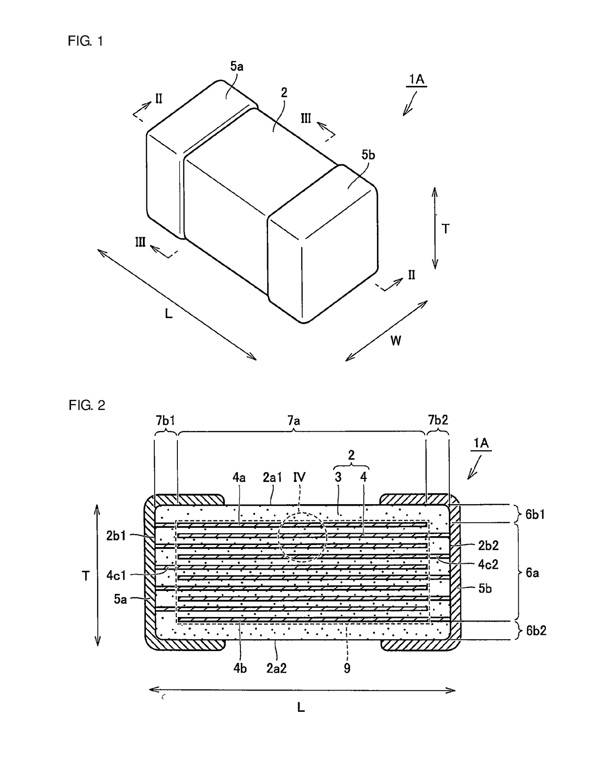
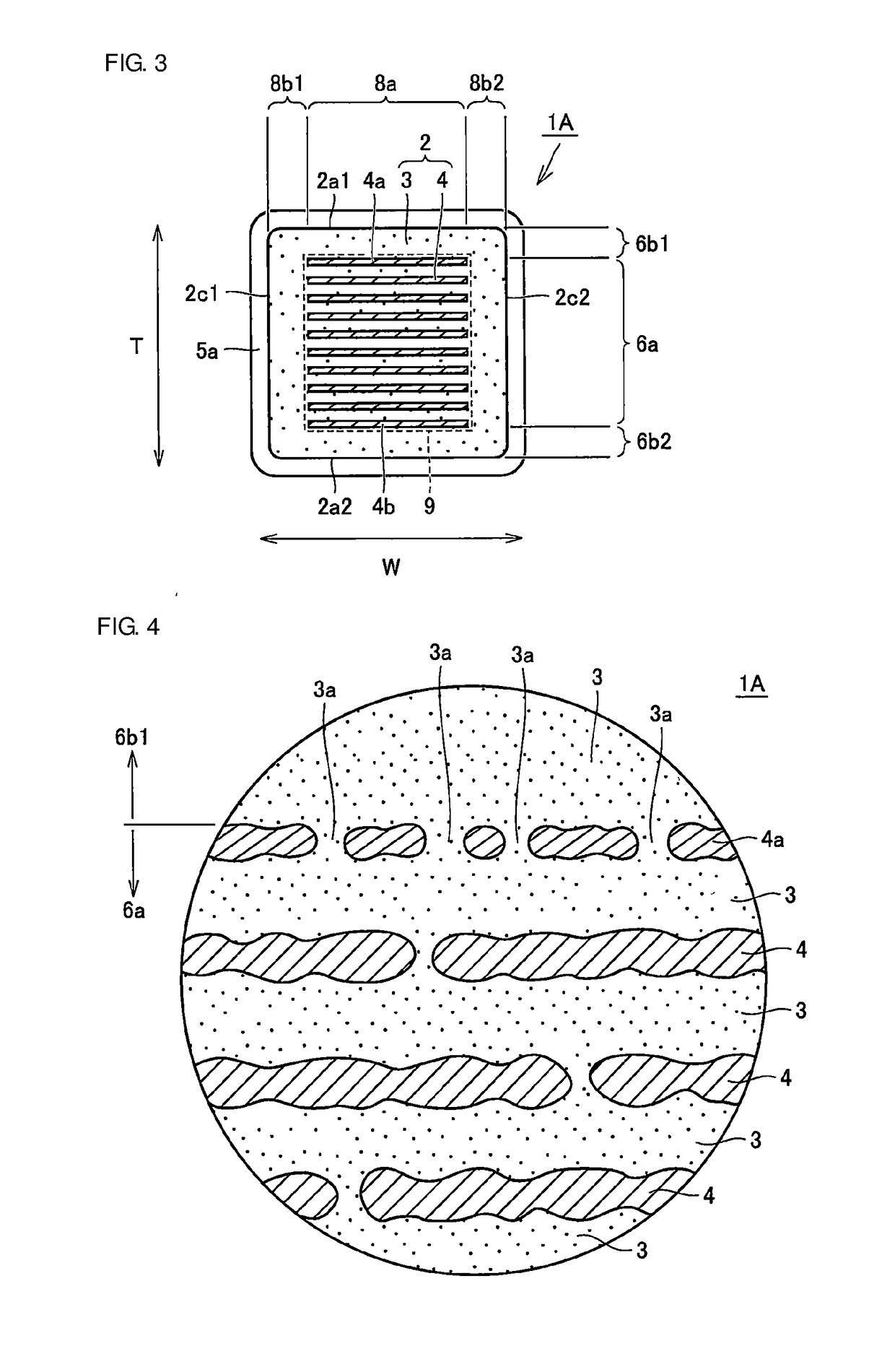
[0039]FIG. 1 is a schematic perspective view of a monolithic ceramic capacitor according to a first preferred embodiment of the present invention. Also, FIGS. 2 and 3 are schematic cross-sectional views taken along line II-II and line III-III in FIG. 1. FIG. 4 is an enlarged view of region IV in FIG. 2. A configuration of a monolithic ceramic capacitor 1A according to this preferred embodiment is described with reference to FIGS. 1 to 4.

[0040]As shown in FIGS. 1 to 3, the monolithic ceramic capacitor 1A is an electronic component having a rectangular or substantially rectangular parallelepiped shape, and includes an element body 2, and a first outer electrode 5a and a second outer electrode 5b defining a pair of outer electrodes.

[0041]As shown in FIGS. 2 and 3, the element body 2 has a rectangular or substantially rectangular parallelepiped shape, and includes ceramic dielectric layers 3 and inner electrode layers 4 defining and serving as conductor layers alternately stacked in a p...

second preferred embodiment

[0104]FIG. 8 is a schematic cross-sectional view of a monolithic ceramic capacitor according to a second preferred embodiment of the present invention. Also, FIGS. 9 and 10 are enlarged views of region IX and region X shown in FIG. 8. First, a configuration of a monolithic ceramic capacitor 1C according to this preferred embodiment is described with reference to FIGS. 8 to 10.

[0105]As shown in FIGS. 8 to 10, the monolithic ceramic capacitor 1C according to this preferred embodiment differs from the monolithic ceramic capacitor 1A according to the above-described first preferred embodiment in the configuration of the inner electrode layer 4, and more specifically, in that a portion of the plurality of inner electrode layers 4 having a lower conductor density than the conductor density of the other portion is different from that portion of the monolithic ceramic capacitor 1A according to the above-described first preferred embodiment.

[0106]In the monolithic ceramic capacitor 1C accord...

third preferred embodiment

[0124]FIG. 12 is a schematic cross-sectional view of a monolithic ceramic capacitor according to a third preferred embodiment of the present invention. FIGS. 13 and 14 are enlarged views of region XIII and region XIV shown in FIG. 12. A configuration of a monolithic ceramic capacitor 1D according to this preferred embodiment is described with reference to FIGS. 12 to 14.

[0125]As shown in FIGS. 12 to 14, the monolithic ceramic capacitor 1D according to this preferred embodiment differs from the monolithic ceramic capacitor 1A according to the above-described first preferred embodiment in the configuration of the inner electrode layer 4, and more specifically, in that a portion of the plurality of inner electrode layers 4 having a lower conductor density than the conductor density of the other portion is different from that portion of the monolithic ceramic capacitor 1A according to the first preferred embodiment.

[0126]In the monolithic ceramic capacitor 1D according to this preferred...


PUM

PropertyMeasurementUnit
thicknessaaaaaaaaaa
thicknessaaaaaaaaaa
distanceaaaaaaaaaa

Abstract

A monolithic ceramic capacitor includes an element body having therein a multilayer portion formed of a plurality of conductor layers and a plurality of ceramic dielectric layers alternately stacked in a thickness direction; and a first outer electrode and a second outer electrode provided on an outer portion of the element body. The element body is divided in the thickness direction into a thickness-direction first outer layer portion, a thickness-direction second outer layer portion, and a thickness-direction inner layer portion located between the thickness-direction first outer layer portion and the thickness-direction second outer layer portion and including the multilayer portion. A first conductor layer and a second conductor layer, which are outermost layers among the plurality of conductor layers, have lower conductor densities than any of conductor densities of the other conductor layers.

Description

BACKGROUND OF THE INVENTION[0001]1. Field of the Invention[0002]The present invention relates to a monolithic ceramic capacitor, which is a type of capacitor element, and which includes a dielectric layer made of a ceramic dielectric material.[0003]2. Description of the Related Art[0004]A capacitor element generally includes an element body, in which conductor layers and dielectric layers are alternately stacked, and an outer electrode provided on an outer surface of the element body. A monolithic ceramic capacitor is a type of capacitor element, in which the dielectric layers are made of a ceramic dielectric material.[0005]The monolithic ceramic capacitor typically includes therein a substantially rectangular-parallelepiped-shaped multilayer portion, in which a plurality of conductor layers defining inner electrode layers and a plurality of ceramic dielectric layers are alternately densely stacked. The multilayer portion is covered with an outer layer portion made of ceramic dielec...

Claims


Application Information

Patent Timeline
Patent Type & Authority Applications(United States)
IPC IPC(8): H01G4/30H01G4/012H01G4/232H01G4/12
CPCH01G4/30H01G4/232H01G4/012H01G4/12
Inventor TAKASHIMA, HIROKAZUSAKAI, SATOKI
Owner MURATA MFG CO LTD
Why Eureka
Try Eureka