AI technical title is built by Patsnap AI team. It summarizes the technical point description of the patent document.
a technology of etching substrate and loadlock, which is applied in the direction of electrical apparatus, basic electric elements, electric discharge tubes, etc., can solve the problems of reducing device yield, affecting device yield, and limiting the success of shadow ring based approach in creating bevel edge exclusion lengths less than . the effect of reducing the exclusion
Active Publication Date: 2017-03-30
APPLIED MATERIALS INC
View PDF3 Cites 10 Cited by
Summary
Abstract
Description
Claims
Application Information
AI Technical Summary
This helps you quickly interpret patents by identifying the three key elements:
Problems solved by technology
Method used
Benefits of technology
Benefits of technology
This patent introduces systems and methods for reducing a "bevel edge exclusion" in the manufacturing of electronic devices. By using a centered mask and a gas flow between the mask and the substrate surface, etchants are delivered to the edge of the substrate while minimizing damage to the substrate under the mask. This results in a more precise and efficient process for manufacturing electronic devices.
Problems solved by technology
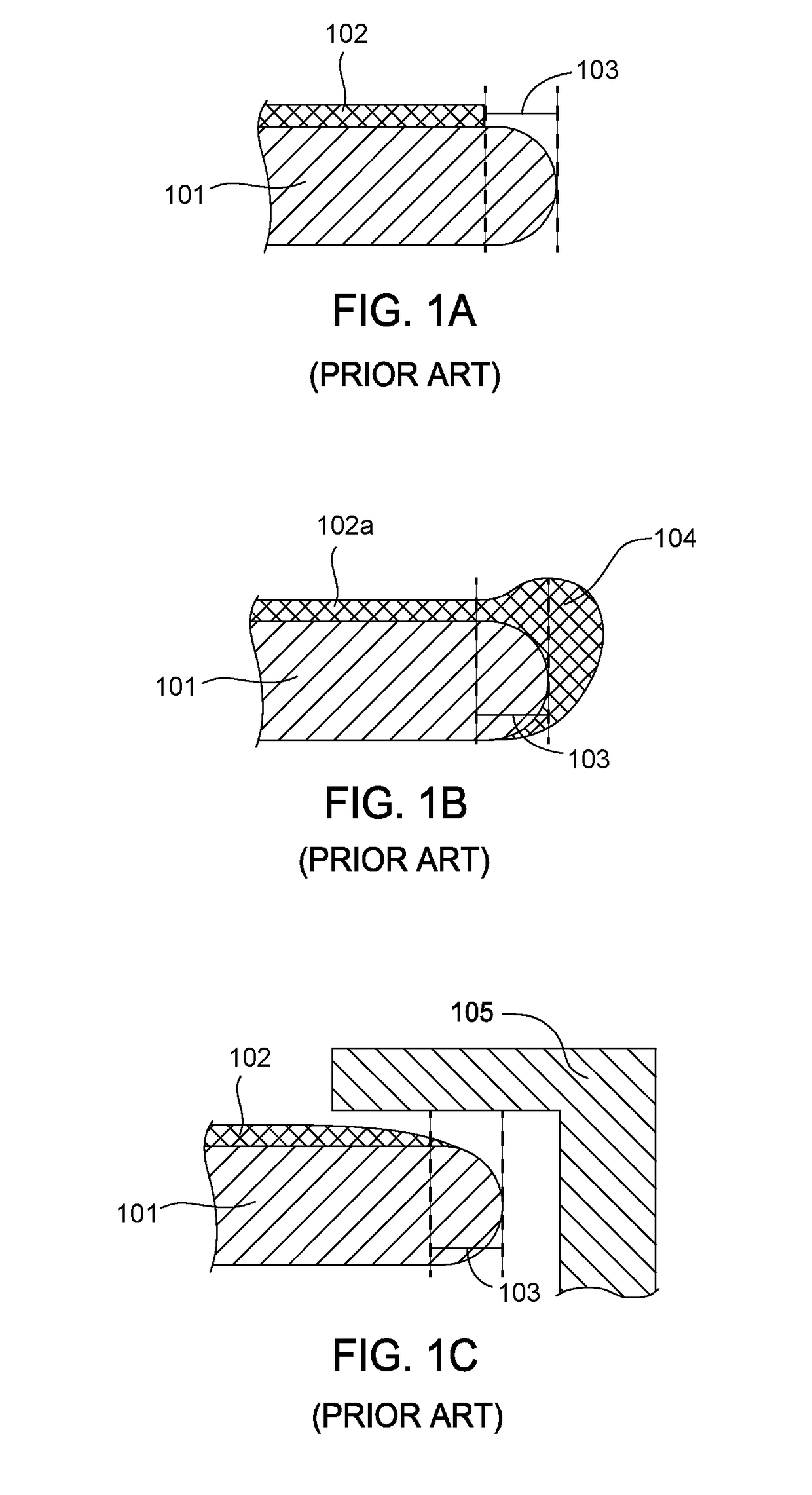
However, due to plasma behavior at the bevel edge of the wafer for some deposition materials such as amorphous carbon, the film can be thicker at the edge resulting in an “edge-hump”.
The limitation of this approach is that the edge exclusion zone extends to 3.5 mm and is detrimental to device yield.
The edge profile is also not easily customizable as it is dependent on the size and shape of the shadow ring.
The current shadow ring based approach has had only limited success creating bevel edge exclusion lengths of less than 3.5 mm.
Method used
Image
Click on the blue label to locate the original text in one second.
Reading with bidirectional positioning of images and text.
Examples
Embodiment Construction
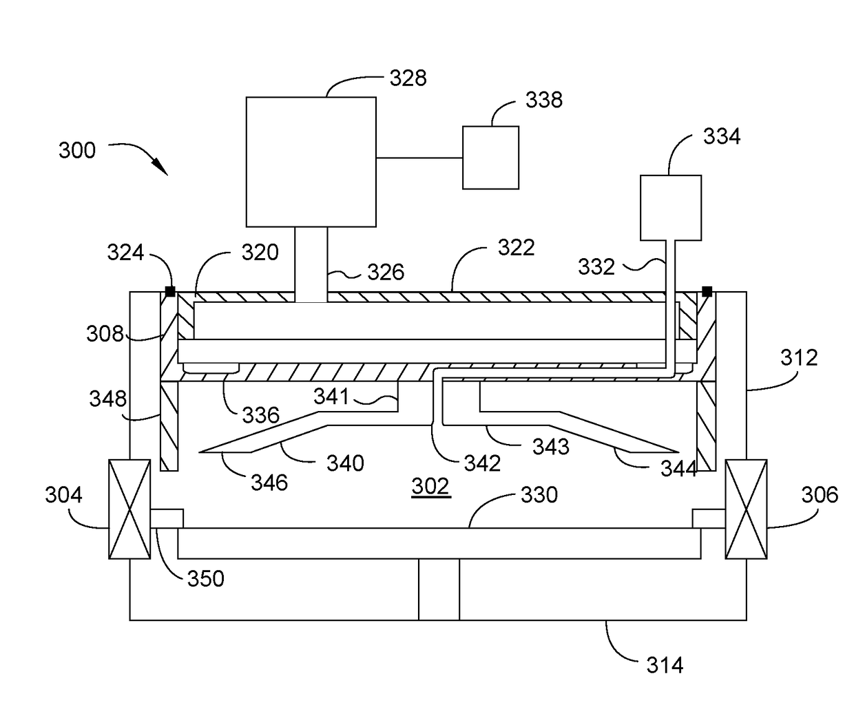
[0025]Implementations disclosed herein describe a bevel etch apparatus located in loadlock bevel etch chamber. The bevel etch system is placed in a process capable loadlock bevel etch chamber and thus does not replace a process chamber and reduce throughput of the deposition tool. The bevel etch apparatus uses a Remote Plasma Source (RPS) to produce oxygen-argonplasma to rapidly etch the bevel edge region of the wafer uniformly along the circumference of the wafer. The etch gas is a mixture of
[0026]Oxygen, Argon, and Nitrogen that is uniformly distributed using a showerhead kind of apparatus. A secondary Argon gas flow is used as the purge gas to control the etch profile and prevent radial diffusion of the etch reactants. During substrate processing, the purge gas flows through a narrow gap between the substrate and the mask.
[0027]The bevel etch apparatus provides customized bevel thickness profiles to meet different customer specifications. The system described herein can clear th...
PUM
Abstract
Implementations disclosed herein describe a bevel etch apparatus within a loadlock bevel etch chamber and methods of using the same. The bevel etch apparatus has a maskassembly within the loadlock bevel etch chamber. During an etch process, the maskassembly delivers a gas flow to control bevel etch without the use of a shadow frame. As such, the edge exclusion at the bevel edge can be reduced, thus increasing product yield.
Description
CROSS-REFERENCE TO RELATED APPLICATIONS[0001]This application claims priority to U.S. Provisional Patent Application Ser. No. 62 / 232,163 (Attorney Docket No. 023433 / USL), filed Sep. 24, 2015, which is incorporated by reference herein.BACKGROUND[0002]Field[0003]Implementations of the present disclosure generally relate to apparatus for etching of substrates during semiconductor manufacturing.[0004]Description of the Related Art[0005]Chip manufacturers strive for high device yield, low defect count, and increased performance from every wafer processed for increased efficiency. Device yield per wafer can be increased by maximizing patterned area on each substrate while maintaining or reducing defect count.[0006]The bevel edge of the wafer needs to be cleaned to avoid bevel peeling and reduce defect count and further contamination of the wafer in the lithography tool. The area near the bevel edge where no deposition is desired to avoid bevel peeling is termed “edge-exclusion”. The depos...
Claims
Application Information
Patent Timeline
Application Date:The date an application was filed.
Publication Date:The date a patent or application was officially published.
First Publication Date:The earliest publication date of a patent with the same application number.
Issue Date:Publication date of the patent grant document.
PCT Entry Date:The Entry date of PCT National Phase.
Estimated Expiry Date:The statutory expiry date of a patent right according to the Patent Law, and it is the longest term of protection that the patent right can achieve without the termination of the patent right due to other reasons(Term extension factor has been taken into account ).
Invalid Date:Actual expiry date is based on effective date or publication date of legal transaction data of invalid patent.
Patent Type & AuthorityApplications(United States)

