Insulated gate type switching device and method for manufacturing the same

Active Publication Date: 2017-03-30
TOYOTA JIDOSHA KK
View PDF0 Cites 2 Cited by
  • Summary
  • Abstract
  • Description
  • Claims
  • Application Information

AI Technical Summary

Benefits of technology

This patent describes a technology for preventing the variation in gate threshold of insulated gate type switching devices that includes a connection region. By implanting p-type impurities to the longitudinal side surfaces of the gate trenches at an inclined angle and setting the semiconductor substrate so that the irradiation direction of the p-type impurities and the short directional side surfaces of the gate trenches are parallel, the p-type impurities are suppressed from being implanted to the short directional side surfaces of the gate trenches. However, the p-type impurities are implanted by a certain amount to entireties of the short directional side surfaces of the gate trenches, which results in a density of the p-type impurities increasing in that range as a result of the irradiation direction and density of the p-type impurities. This technology prevents the gate threshold from widely varying during mass-production of the MOSFETs.

Problems solved by technology

However, it is difficult to accurately set the semiconductor substrate so that the irradiation direction of the p-type impurities and the short directional side surfaces are parallel.
Due to this, the technology of Japanese Patent Application Publication No. 2015-118966 has a problem in that the gate threshold widely varies at the time of mass-production of the MOSFETs.

Method used


Image

  • Insulated gate type switching device and method for manufacturing the same
  • Insulated gate type switching device and method for manufacturing the same
  • Insulated gate type switching device and method for manufacturing the same

Examples


Embodiment Construction

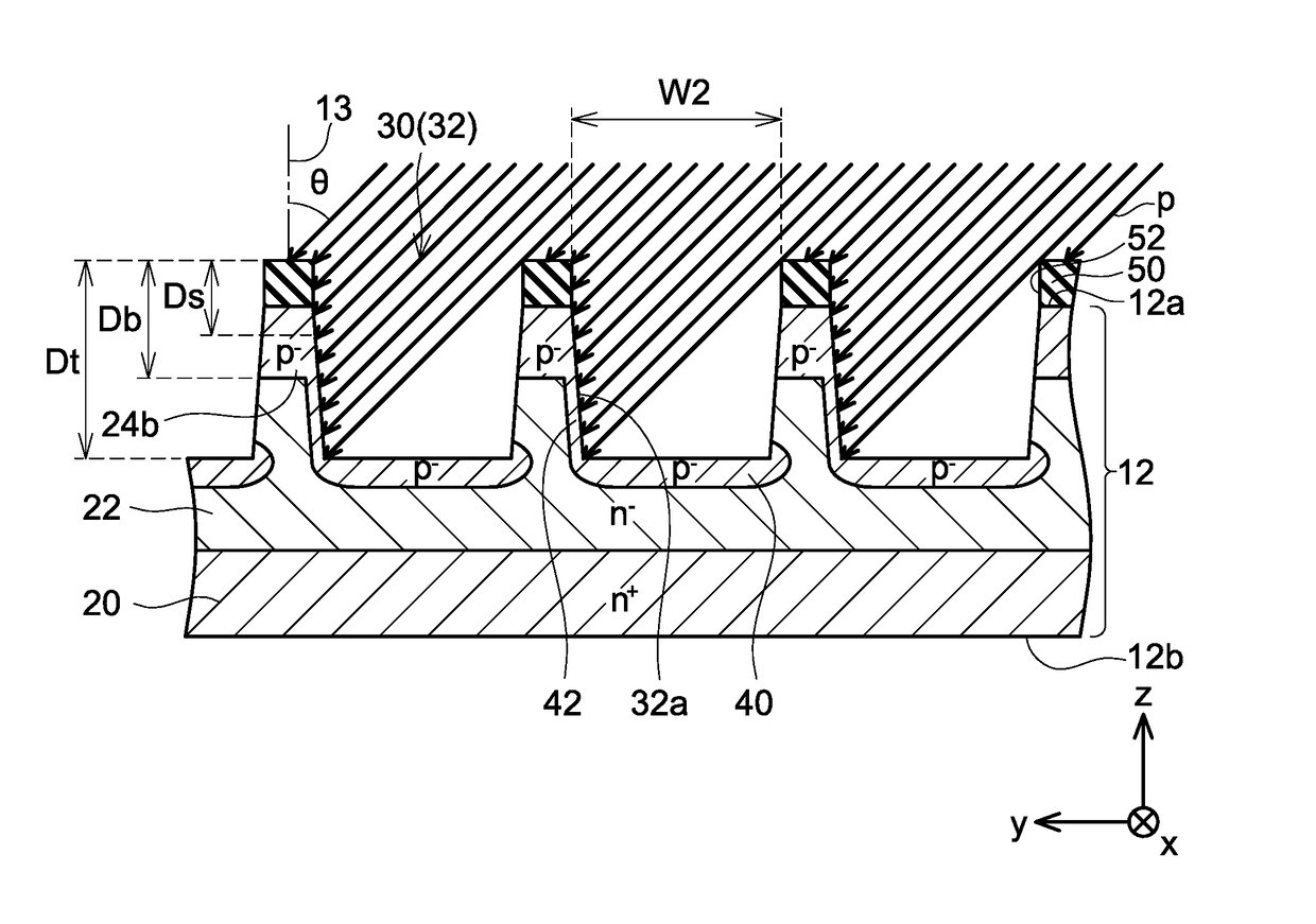
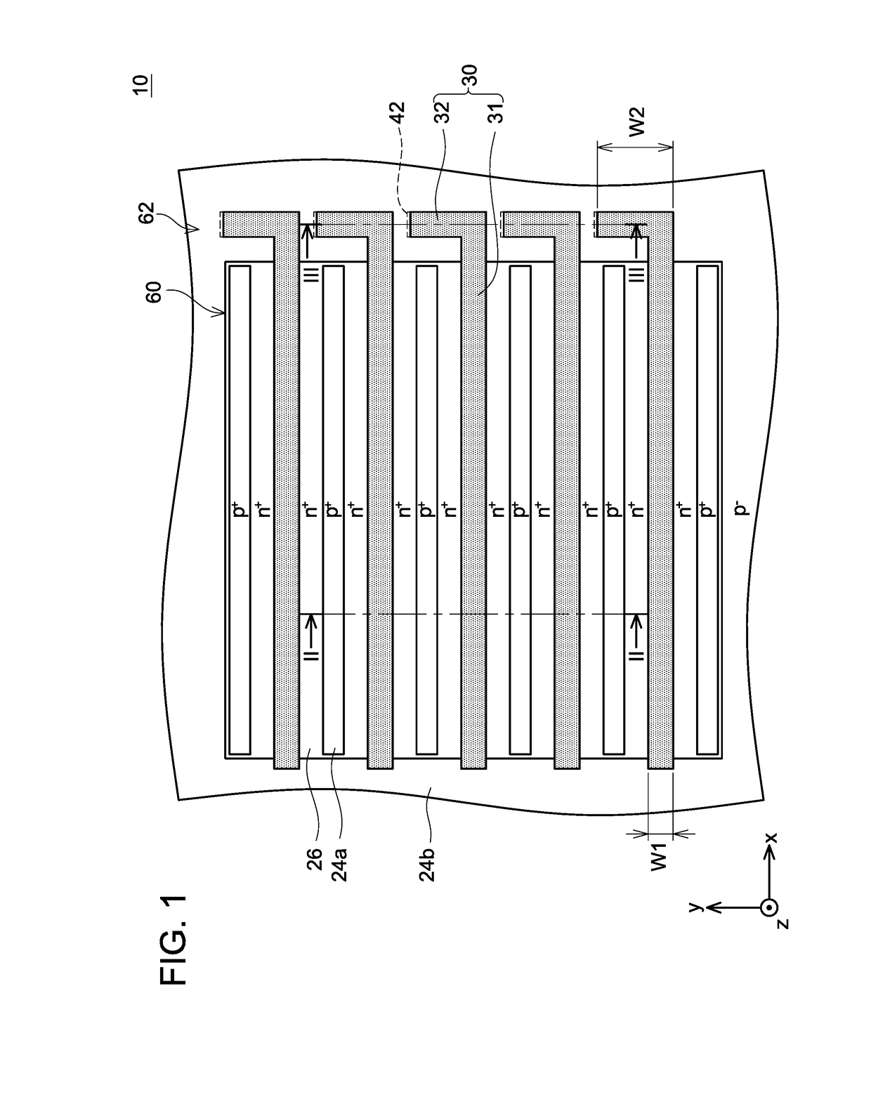
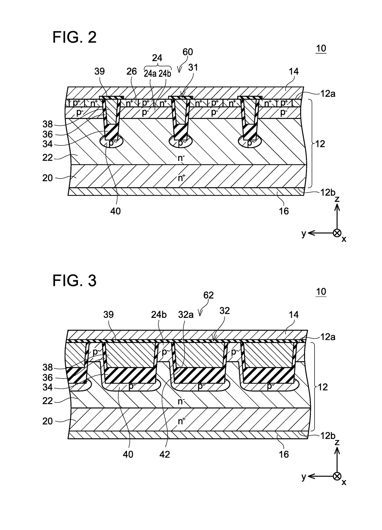
[0033]As shown in FIGS. 2 and 3, a MOSFET 10 according to an embodiment comprises a semiconductor substrate 12, an upper electrode 14, and a lower electrode 16. The semiconductor substrate 12 is made of SiC. The upper electrode 14 covers an upper surface 12a of the semiconductor substrate 12. The lower electrode 16 covers a lower surface 12b of the semiconductor substrate 12. Note that, herein, a thickness direction of the semiconductor substrate 12 is referred to as a z-direction, one direction orthogonal to the z-direction (one direction parallel to the upper surface 12a) is referred to as an x-direction, and a direction orthogonal to both the z-direction and the x-direction is referred to as a y-direction.

[0034]As shown in FIG. 1, in the semiconductor substrate 12, source regions 26 and body contact regions 24a are located in a manner of being exposed on the upper surface 12a of the semiconductor substrate 12. In the following, a range where the source regions 26 and the body con...


PUM


Abstract

A method of manufacturing an insulated gate type switching device includes forming a gate trench that has a first portion with a first width in a first direction and a second portion with a second width in the first direction, the second width being wider than the first width. In an oblique implantation, second conductivity type impurities are irradiated at an irradiation angle inclined around an axis orthogonal to the first direction. The first width, the second width, and the irradiation angle are set such that the second conductivity type impurities are suppressed, at a first side surface of the first portion, from being. implanted into a part below a lower end of a second semiconductor region, and at a second side surface of the second portion, the impurities are implanted into the part below the lower end of the second semiconductor region.

Description

CROSS-REFERENCE TO RELATED APPLICATION[0001]This application claims priority to Japanese Patent Application No. 2015-186613 filed on Sep. 24, 2015, the entire contents of which are hereby incorporated by reference into the present application.TECHNICAL FIELD[0002]The present application relates to an insulated gate type switching device and a method. for manufacturing the same. Note that, the insulated gate type switching device herein refers to a switching device including a gate electrode insulated from a semiconductor substrate. As examples of the insulated gate type switching device, there are given a MOSFET and an IGBT.DESCRIPTION OF RELATED ART[0003]A MOSFET disclosed in Japanese Patent Application Publication No. 2015-118966 includes a laminated structure including an n-type drift region, a p-type body region, and an n-type source region. In a surface of a semiconductor substrate, gate trenches penetrating the source region and the body region so as to reach the drift region ...

Claims


Application Information

Patent Timeline
IPC IPC(8): H01L29/66H01L29/739H01L29/78H01L29/10
CPCH01L29/66734H01L29/1095H01L29/66348H01L29/7813H01L29/7397H01L21/26513H01L21/26586H01L21/26506H01L29/4238H01L29/0623H01L29/0696
Inventor ONISHI, TORUONOGI, ATSUSHIMISUMI, TADASHIYAMASHITA, YUSUKETAKEUCHI, YUICHI
Owner TOYOTA JIDOSHA KK
Why Eureka
Try Eureka