Method of making nonvolatile semiconductor memory
a semiconductor memory and non-volatile technology, applied in semiconductor devices, instruments, electrical apparatus, etc., can solve the problems of large power consumption at writing, inability to employ the virtual ground method of fn tunnel current for writing, and poor electron injection efficiency (write efficiency) efficiency, so as to reduce the electric field applied, prevent the tunnel phenomenon from occurring, and reduce the thickness
- Summary
- Abstract
- Description
- Claims
- Application Information
AI Technical Summary
Benefits of technology
Problems solved by technology
Method used
Image

Examples
example 1
(EXAMPLE 1)
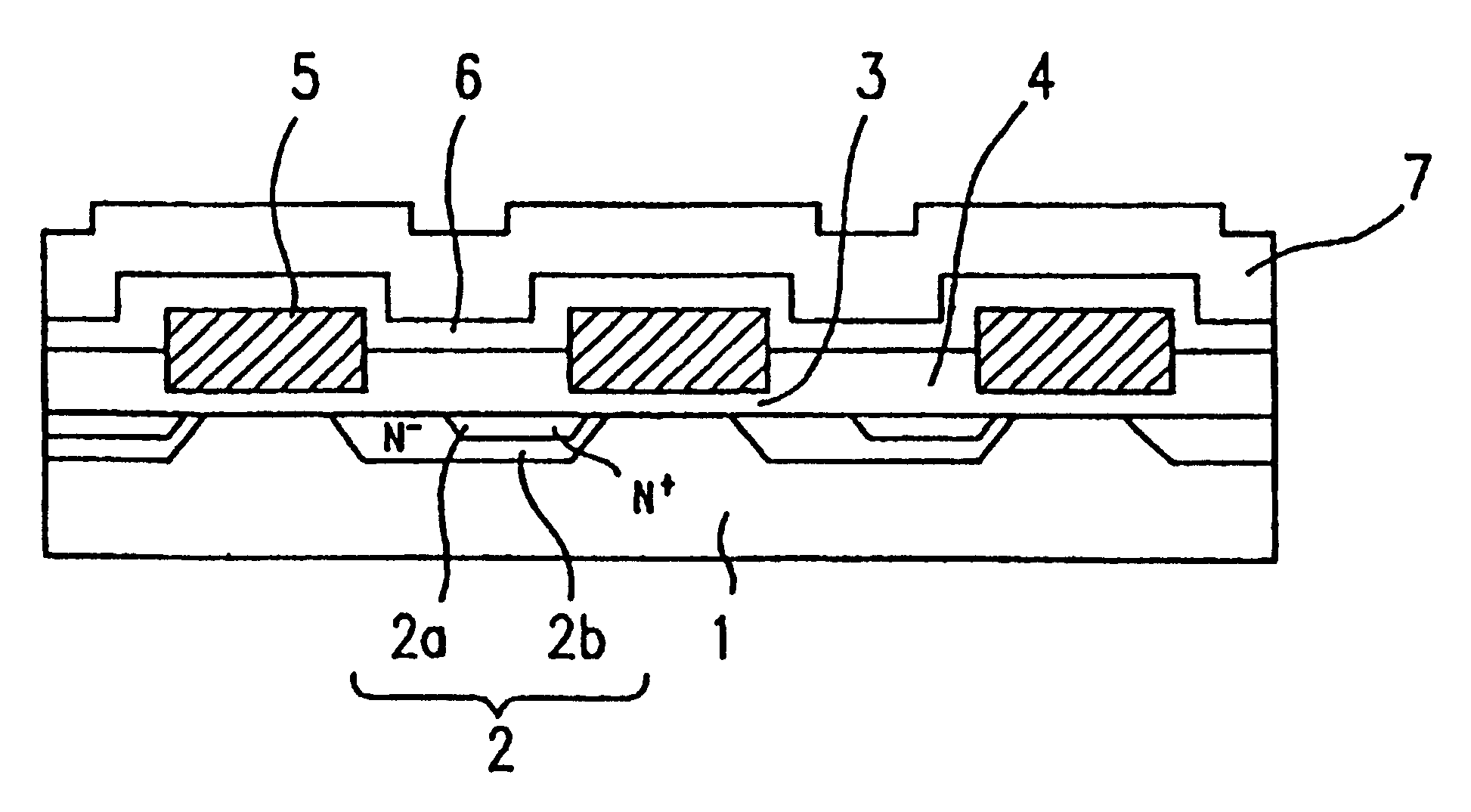
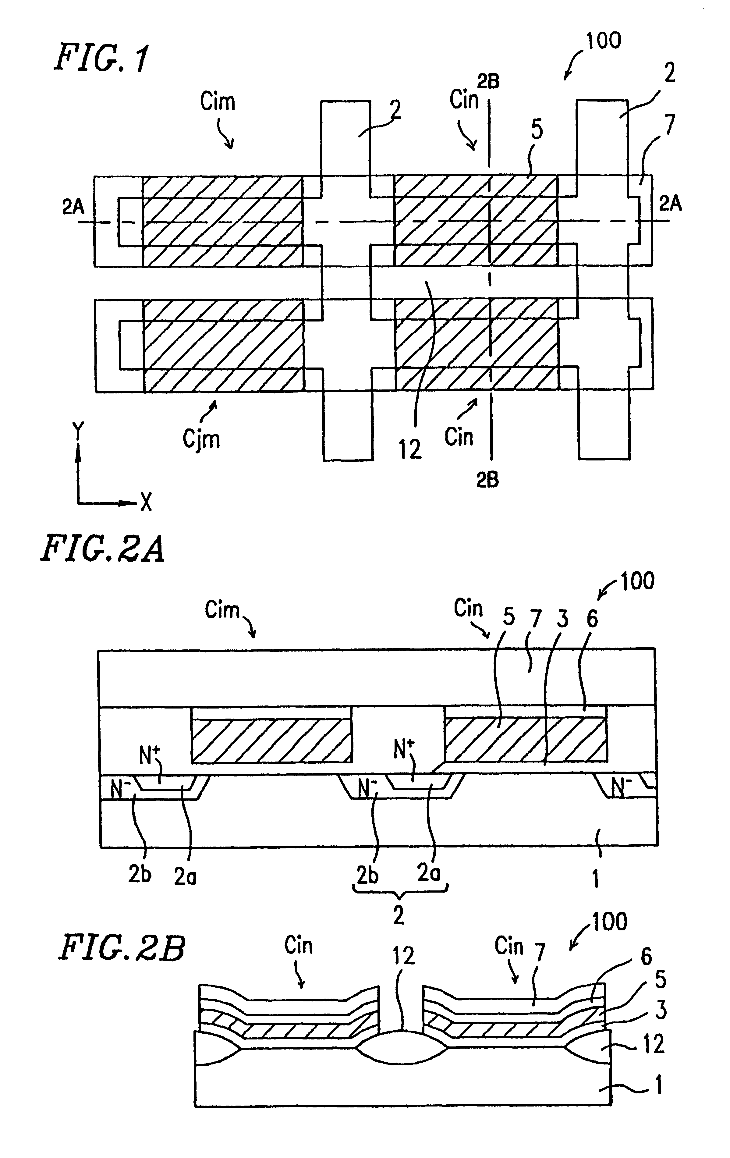
FIG. 1 is a plan view of a portion of a memory cell array of a nonvolatile semiconductor memory 100 of Example 1 according to the present invention. FIGS. 2A and 2B are sectional views of the nonvolatile semiconductor memory 100 taken along lines A--A and B--B of FIG. 1, respectively,
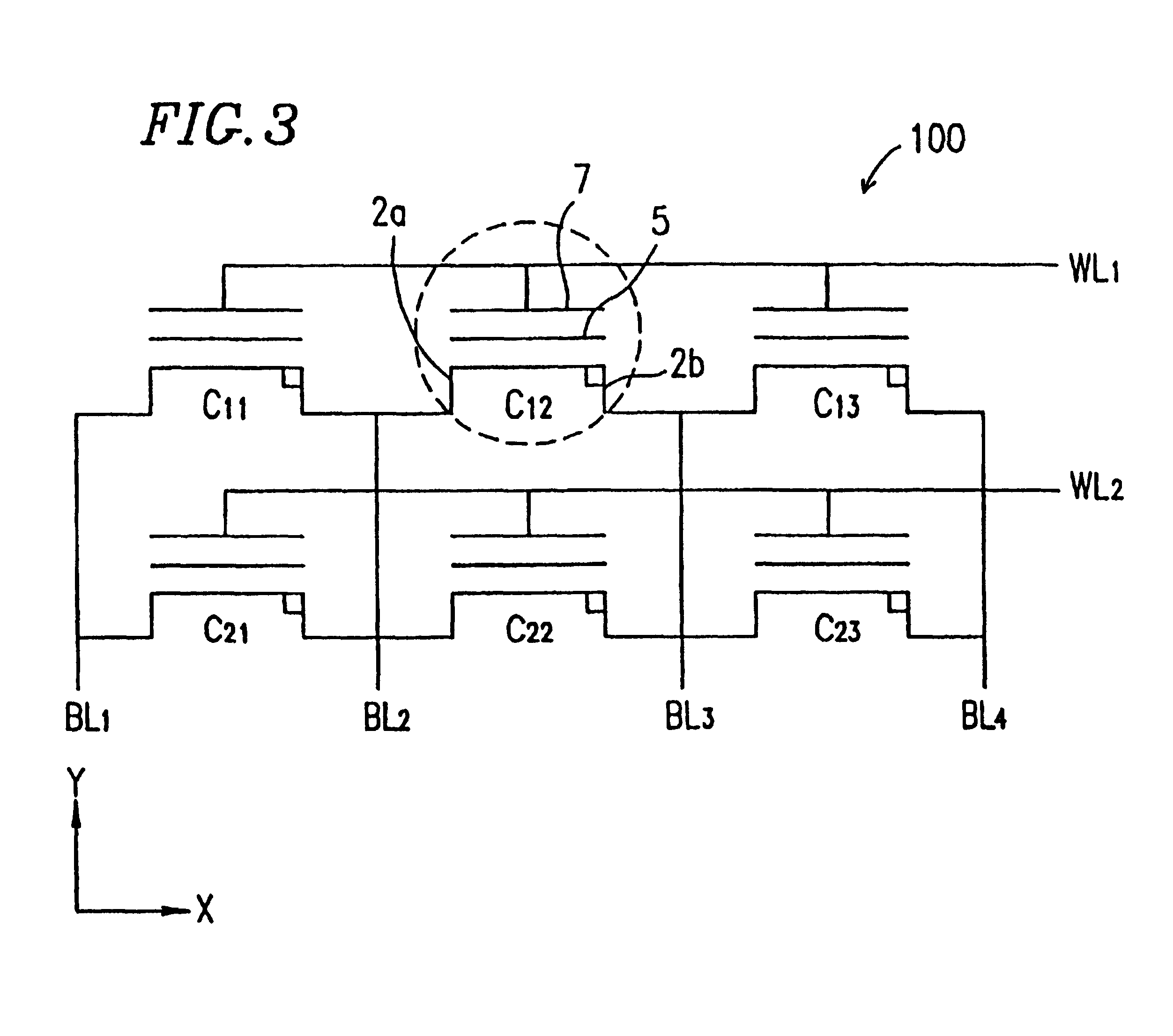
Referring to FIGS. 1, 2A, and 2B, the nonvolatile semiconductor memory 100 includes a plurality of memory cells C formed in a matrix on a semiconductor substrate 1. In FIG. 1, the respective memory cells C are denoted by individual codes such as C.sub.im. Each of the memory cells C includes a tunnel insulating film 3 formed on the semiconductor substrate 1 and a floating gate 5 formed on the tunnel insulating film 3.
A control gate 7 is formed on the floating gate 5 via an insulating film 6 made of ONO and the like. Such control gates 7 extend in a channel direction of the memory cell C (an X direction shown in FIG. 1), constituting a word line WL as shown in FIG. 3 for connecting the memory c...
example 2
(EXAMPLE 2)
Referring to FIGS. 6 to 10, a first example of the fabrication method of a nonvolatile semiconductor memory according to the present invention will be described. In this example, the fabrication method of the nonvolatile semiconductor memory 100 of Example 1 will be described. FIGS. 6 to 10 are sectional views taken along line A--A of FIG. 1, showing steps of the fabrication method.
First, the field insulating films (element isolation films) 12 shown in FIG. 2B are formed on the semiconductor substrate (silicon substrate) 1. Then, the tunnel insulating film 3 with a thickness of about 80 .ANG. is formed by thermal oxidation, and first polysilicon is deposited on the tunnel insulating film 3 to a thickness of about 1000 to 2000 .ANG.. A first resist mask 8a with a predetermined pattern is formed on the first polysilicon by photolithography, to form first polysilicon layers 5' in a striped shape by patterning. Each of the first polysilicon layers 5' has the same width as the...
example 3
(EXAMPLE 3)
FIG. 14 is a plan view of a portion of a memory cell array of a nonvolatile semiconductor memory 300 of Example 4 according to the present invention. FIGS. 15A and 15B are sectional views of the nonvolatile semiconductor memory 300 taken along lines A--A and B--B of FIG. 14, respectively,
Referring to FIGS. 14, 15A, and 15B, the nonvolatile semiconductor memory 300 includes a plurality of memory cells C' formed in a matrix on a semiconductor substrate 31. In FIG. 14, the respective memory cells C' are denoted by individual codes such as C'.sub.im. Each of the memory cells C' includes a floating gate 35 formed on the semiconductor substrate 31 via an insulating film. A control gate 37 is formed on the floating gate 35 via an insulating film 36 made of ONO and the like. Such control gates 37 extend in a channel direction of the memory cell C' (an X direction shown in FIG. 14), constituting a word line WL as shown in FIG. 16 for connecting the memory cells C' lined in the X d...
PUM
 Abstract
Description
Claims
Application Information
 - R&D Engineer
- R&D Manager
- IP Professional
- Industry Leading Data Capabilities
- Powerful AI technology
- Patent DNA Extraction
Browse by: Latest US Patents, China's latest patents, Technical Efficacy Thesaurus, Application Domain, Technology Topic.
© 2024 PatSnap. All rights reserved.Legal|Privacy policy|Modern Slavery Act Transparency Statement|Sitemap