
Magneto-resistance random access memory device and method of manufacturing the same

a random access and memory device technology, applied in the direction of galvano-magnetic device manufacturing/treatment, magnetic field-controlled resistors, material selection of galvano-magnetic materials, etc., can solve the problems of electrical short between the two magnetic substances, electrical short may occur, etc., to prevent the electrical short of the magnetic tunnel junction (mtj) pattern

Active Publication Date: 2017-03-30
SAMSUNG ELECTRONICS CO LTD
View PDF11 Cites 26 Cited by
  • Summary
  • Abstract
  • Description
  • Claims
  • Application Information

AI Technical Summary

Benefits of technology

Example inventive concepts provide a MRAM device that can prevent short circuits in the MTJ pattern and also prevent a decrease in the magnetic properties of the MTJ pattern.

Problems solved by technology

The re-deposited etch residues may cause an electrical short between the two magnetic substances.
In some cases, an electrical short may occur, despite the oxidation process, due to non-oxide etch residues and a non-uniformity of the amounts of the etch residue.

Method used


Image

  • Magneto-resistance random access memory device and method of manufacturing the same
  • Magneto-resistance random access memory device and method of manufacturing the same
  • Magneto-resistance random access memory device and method of manufacturing the same

Examples


Embodiment Construction

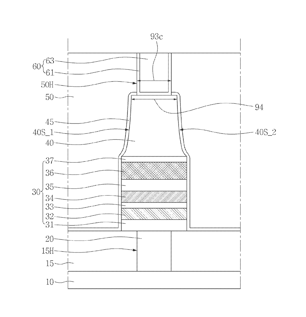
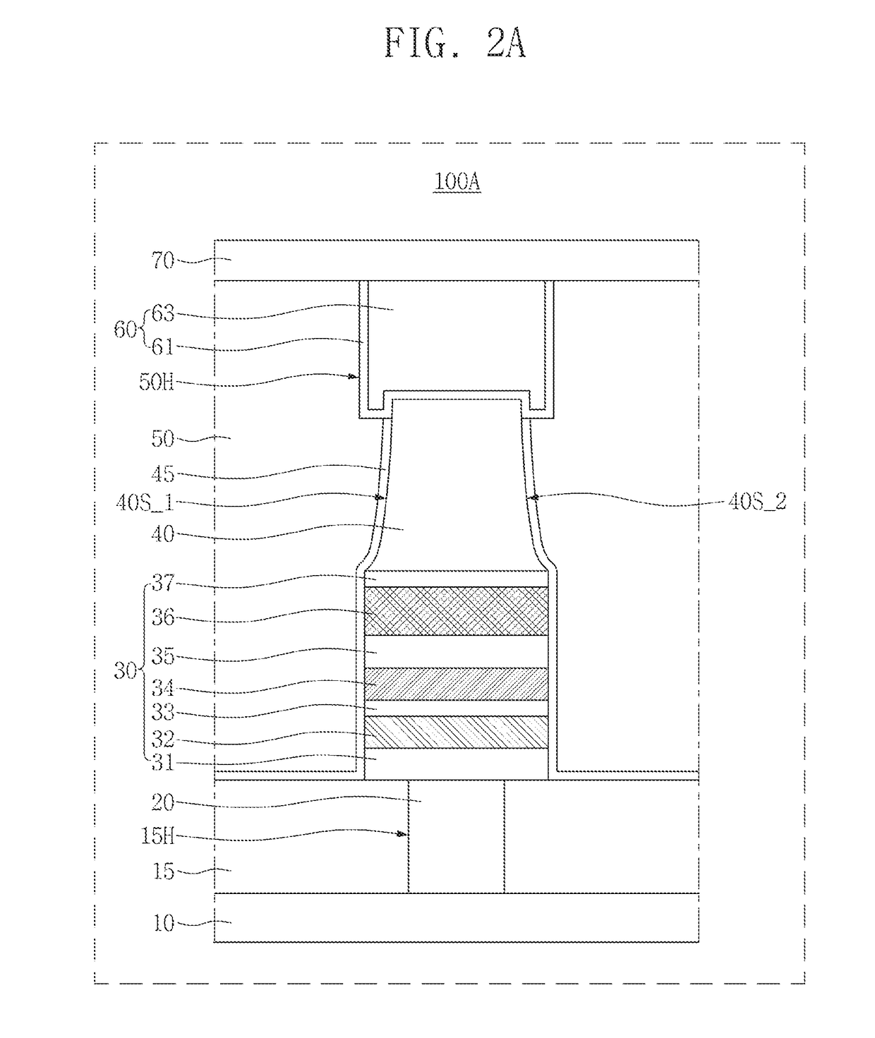
[0023]Example embodiments will now be described more fully with reference to the accompanying drawings, in which some example embodiments are shown. Example embodiments, may, however, be embodied in many different forms and should not be construed as being limited to the embodiments set forth herein; rather, these example embodiments are provided so that this disclosure will be thorough and complete, and will fully convey the scope of example embodiments of inventive concepts to those of ordinary skill in the art. In the drawings, the thicknesses of layers and regions are exaggerated for clarity. Like reference characters and / or numerals in the drawings denote like elements, and thus their description may not be repeated.

[0024]The terminology used herein to describe embodiments of inventive concepts is not intended to limit the scope of inventive concepts. The articles “a,”“an,” and “the” are singular in that they have a single referent; however, the use of the singular form in the ...


PUM


Abstract

Manufacturing a MRAM device may include removing etch residues from a magnetic tunnel junction (MTJ) pattern in the presence of an atmosphere. The removing may include applying a cleaning solution to one or more surfaces of the MTJ pattern. Manufacturing the MRAM device may include removing an oxide layer based on sputter etching of the MTJ pattern. The etch residues may be removed such that the oxide layer is formed. Removing the etch residues may include applying a cleaning solution to the MTJ pattern. The etch residues may be removed in the presence of an atmosphere. The MTJ pattern may be formed based on patterning an MTJ layer in a vacuum state such that the etch residues are formed on a surface of the MTJ pattern.

Description

CROSS-REFERENCE TO RELATED APPLICATION[0001]This application claims priority under 35 U.S.C. §119 to Korean Patent Application No. 10-2015-0137929 filed on Sep. 30, 2015, the disclosure of which is hereby incorporated by reference in its entirety.BACKGROUND[0002]Technical Field[0003]Inventive concepts relate to a magneto-resistance random access memory device and a method of manufacturing the same.[0004]Description of Related Art[0005]Magneto-resistance random access memory (MRAM) devices are non-volatile memory devices that read and / or write using a magnetic tunnel junction (MTJ) pattern having two magnetic substances and an insulating layer interposed between thereof. In a process of manufacturing the MRAM device, the MTJ pattern is patterned by performing a sputter etching process. Etch residues may be generated based on the patterning of the MTJ pattern. The generated etch residues may be re-deposited on sidewalls of the MTJ pattern. The re-deposited etch residues may cause an e...

Claims


Application Information

Patent Timeline
Patent Type & Authority Applications(United States)
IPC IPC(8): H01L43/12H01L43/02H01L43/10H01L43/08H10N50/01H10N50/10H10N50/80
CPCH01L43/12H01L43/10H01L43/02H01L43/08H10N50/01H10N50/10H10N50/80H10N50/85
Inventor LEE, WONJUNHWANG, LNSEAKKO, YONGSUNLEE, CHANGKYUBAE, JINHYESHIN, HYUNCHULHAN, SHINHEEHAN, YOONSUNG
Owner SAMSUNG ELECTRONICS CO LTD
Learn More