Semiconductors compositions for dye-sensitized solar cells

a technology of solar cells and semiconductors, applied in the field of semiconductor compositions, can solve the problems of unusual warming of the earth's atmosphere, non-renewable energy sources of fossil fuels, etc., and achieve the effects of limiting or preventing the airborne of nanoparticles, limiting or preventing adverse environmental or health risks

Inactive Publication Date: 2011-09-29
WARNER BABCOCK INST FOR GREEN CHEM
View PDF0 Cites 4 Cited by
  • Summary
  • Abstract
  • Description
  • Claims
  • Application Information

AI Technical Summary

Benefits of technology

[0007]The present application discloses a semiconductor composition for use in a solar cell, such as a thin film dye-sensitized solar cell. More particularly, embodiments are disclosed in which nanoparticles of semiconductor material are tethered together in a nanonodular network via a multi-functional organic linking compound. The tethered molecules form a nanonodular network of immobilized nanoparticles, thus limiting or preventing the nanoparticles from becoming airborne and limiting or preventing adverse environmental or health risks potentially associated with airborne nanoparticles.

Problems solved by technology

Fossil fuels, however, are non-renewable sources of energy (i.e., energy sources that cannot be recreated by man).
Excessive amounts of greenhouse gases cause unusual warming of the earth's atmosphere, the greenhouse effect, which is a significant environmental concern.

Method used


Image

  • Semiconductors compositions for dye-sensitized solar cells
  • Semiconductors compositions for dye-sensitized solar cells
  • Semiconductors compositions for dye-sensitized solar cells

Examples


example 1

[0048]Particle size measurements for a nanonodular network. The following experiment was performed to demonstrate the formation of nanonodules. First, a dispersion of titanium dioxide nanoparticles was prepared by a sol-gel method. Titanium isopropoxide was added into a 0.075 M solution of nitric acid in deionized water. The dispersion was then hydrolysed by heating it to 80° C. for ten hours. The dispersion was then heated in a sealed pressure tube at 250° C. for twelve hours, which is the step by which porous nanocrystalline (primarily anatase) networks are formed. The resulting dispersion was then sonicated for ten minutes, diluted to approximately 2% solids with deionized water, and pressure filtered using a 200 nm Whatman® Nuclepore™ polycarbonate membrane filter. The filtrate (referred to below as titanium dioxide sol), which contained particles of less than 200 nm, was divided into three equal samples and then used to prepare the following.

[0049]Sample 1 was prepared by addin...

example 2

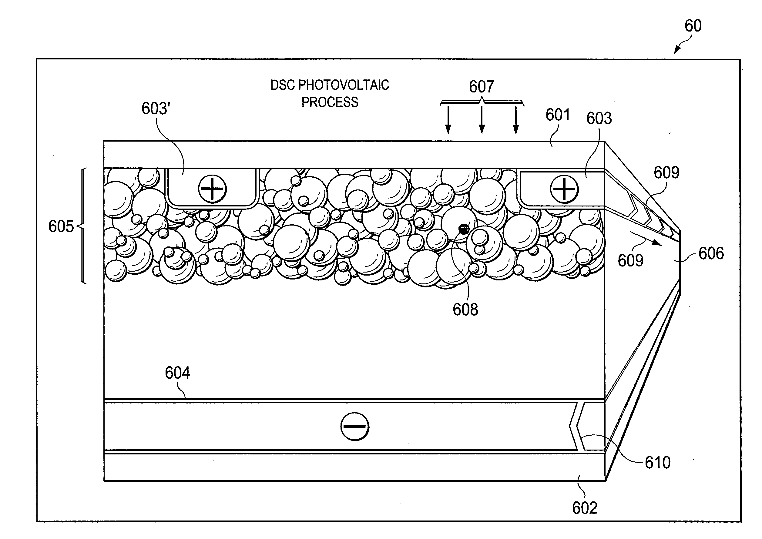
[0052]Performance of a dye-sensitized solar cell having a semiconductor with a nanondular network. This example demonstrates that, in some embodiments, adding a linking compound to form a nanonodular network does not reduce the performance of the solar cell as it would otherwise be absent the linking compound.

[0053]Two titanium dioxide based slurries were prepared as follows. A first slurry was prepared by mixing titanium dioxide nanopowder (Evonik Degussa Corporation, Aeroxide® P25 (“P25”) having an average primary particle size of 21 nm) (about 37% by weight) with water (about 62% by weight) and Triton X-100 (octylphenol ethoxylate sold by the Dow Chemical Company) (about 0.6% by weight). To this mixture was added titanium dioxide nanoparticles synthesized by a sol-gel method (see EXAMPLE 1). A second slurry was prepared the same as the first slurry, except that trimesic acid was added at 0.3% by weight of the P25 TiO2.

[0054]A layer of the first and second slurries were deposited ...


PUM

PropertyMeasurementUnit
average particle diameteraaaaaaaaaa
particle diameteraaaaaaaaaa

Abstract

The present application discloses compositions for thin film dye-sensitized solar cells in which nanoparticles of semiconductor material are tethered together in a nanonodular network using a multi-functional linking compound.

Description

CROSS-REFERENCE TO RELATED APPLICATIONS[0001]This application claims priority to U.S. Provisional Application No. 61 / 305,861, filed Feb. 18, 2010 and entitled, “SEMICONDUCTOR ADDITIVES FOR ELECTRON CHANNELING” [WBI 24.004]; U.S. Provisional Application No. 61 / 305,899, filed Feb. 18, 2010 and entitled, “COMPOSITION OF MATTER FOR SOLAR CELLS” [WBI 24.006]; U.S. Provisional Application No. 61 / 305,908, filed Feb. 18, 2010 and entitled, “NANONODULARITY FOR SEMICONDUCTORS IN SOLAR CELLS” [WBI 24.007]; and U.S. Provisional Application No. 61 / 305,911, filed Feb. 18, 2010 and entitled, “ROOM TEMPERATURE COALESCENCE OF METAL OXIDES FOR SOLAR CELLS” [WBI 24.008], the disclosures of which are hereby incorporated herein by reference.[0002]Further, this application is related to Attorney Docket No. ONEP.P0024US entitled, “ADDITIVES FOR SOLAR CELL SEMICONDUCTORS”; and Attorney Docket No. ONEP.P0025US entitled, “SYSTEMS AND METHODS FOR PREPARING COMPONENTS OF PHOTOVOLTAIC CELLS,” both filed concurr...

Claims


Application Information

Patent Timeline
Patent Type & Authority Applications(United States)
IPC IPC(8): H01L51/46H01L31/18C08G83/00C07F7/28H01L31/042
CPCH01G9/2031Y10T428/2982Y02E10/542H01G9/2059
Inventor WARNER, JOHN C.VAN BENSCHOTEN, HELENCANNON, AMY
Owner WARNER BABCOCK INST FOR GREEN CHEM
Why Eureka
Try Eureka