

Photo-definable glass with integrated electronics and ground plane
a technology of integrated electronics and ground planes, applied in the direction of conductive pattern formation, printed circuit non-printed electric components association, semiconductor/solid-state device details, etc., can solve the problems of high cost and low yield of traditional glass semiconductor microfabrication, and the reliance on expensive capital equipment of semiconductor microfabrication processes
- Summary
- Abstract
- Description
- Claims
- Application Information
AI Technical Summary
Benefits of technology
Problems solved by technology
Method used
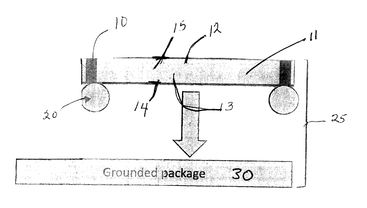
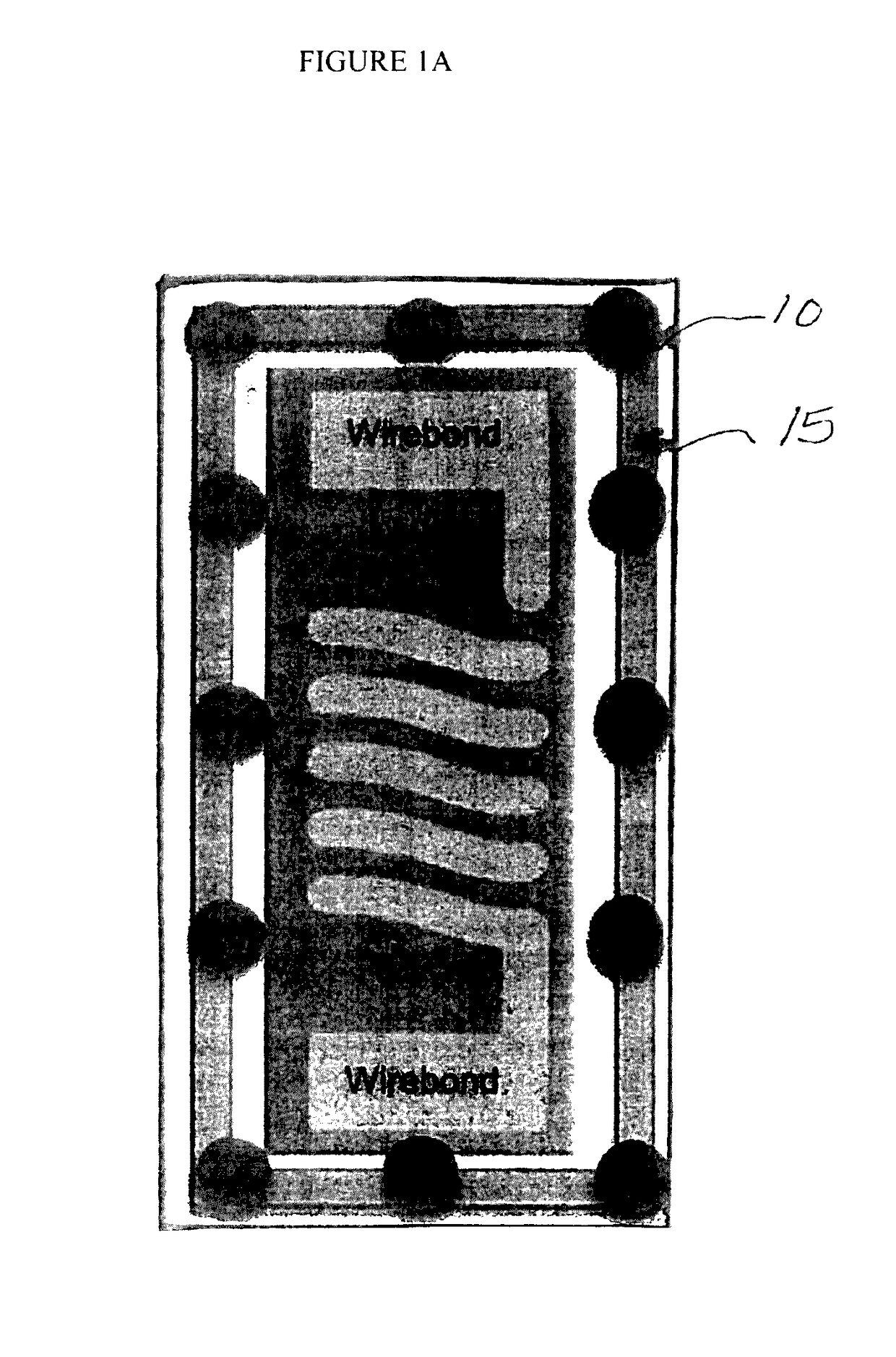
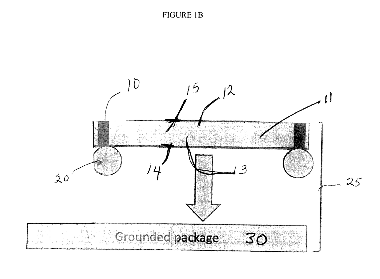
Image

Examples
Embodiment Construction
[0016]While the making and using of various embodiments of the present invention are discussed in detail below, it should be appreciated that the present invention provides many applicable inventive concepts that can be embodied in a wide variety of specific contexts. The specific embodiments discussed herein are merely illustrative of specific ways to make and use the invention and do not delimit the scope of the invention.
[0017]To facilitate the understanding of this invention, a number of terms are defined below. Terms defined herein have meanings as commonly understood by a person of ordinary skill in the areas relevant to the present invention. Terms such as “a”, “an” and “the” are not intended to refer to only a singular entity, but include the general class of which a specific example may be used for illustration. The terminology herein is used to describe specific embodiments of the invention, but their usage does not delimit the invention, except as outlined in the claims.
[...
PUM
 Abstract
Description
Claims
Application Information