Electronic component

a technology of electronic components and components, applied in the field of electronic components, can solve the problems of increasing the resistance value of the electronic component, and achieve the effect of reducing the resistance value and reducing the contact resistan

Active Publication Date: 2017-04-13
MURATA MFG CO LTD
View PDF10 Cites 15 Cited by
  • Summary
  • Abstract
  • Description
  • Claims
  • Application Information

AI Technical Summary

Benefits of technology

[0017]In an electronic component according to a preferred embodiment of the present invention, the electronic component body includes the internal electrode that is partially extended to the surface of the electronic component body and is provided to be connected to the external electrode, the external electrode includes a conductive material-containing resin layer including a conductive material and a resin layer, and a plated layer provided to cover the conductive material-containing resin layer, the conductive material-containing resin layer includes metal particles as the conductive material, and the plated layer extends from the surface of the conductive material-containing resin layer such that the plated layer coats at least some of the metal particles. Thus, the electronic component makes it possible to reduce the contact resistance between the metal particles, thus making the resistance value smaller, as compared with electronic components simply including plated layers on the surfaces of conductive material-containing resin layers.

Problems solved by technology

Thus, the electronic component has the problem of increasing the resistance value, as compared with chip-type electronic components including external electrodes of baked electrodes formed by integrally baking a conductive paste.

Method used


Image

  • Electronic component
  • Electronic component
  • Electronic component

Examples


Embodiment Construction

[0027]Features of the present invention will be described in more detail below with reference to preferred embodiments of the present invention.

[0028]It is to be noted that an example of a multilayer ceramic capacitor will be described as an electronic component in preferred embodiments of the present invention.

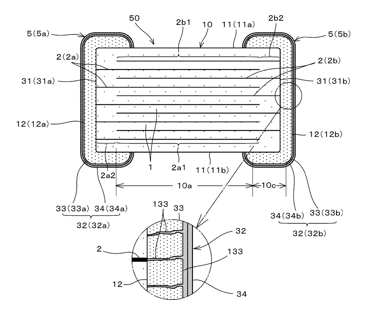
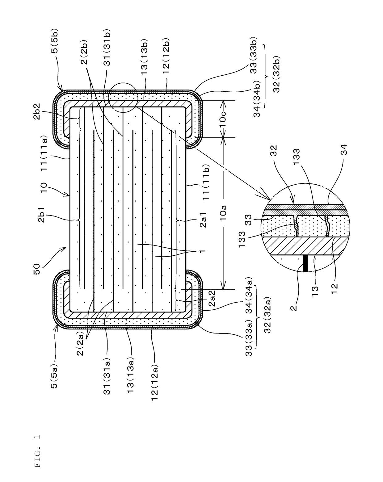
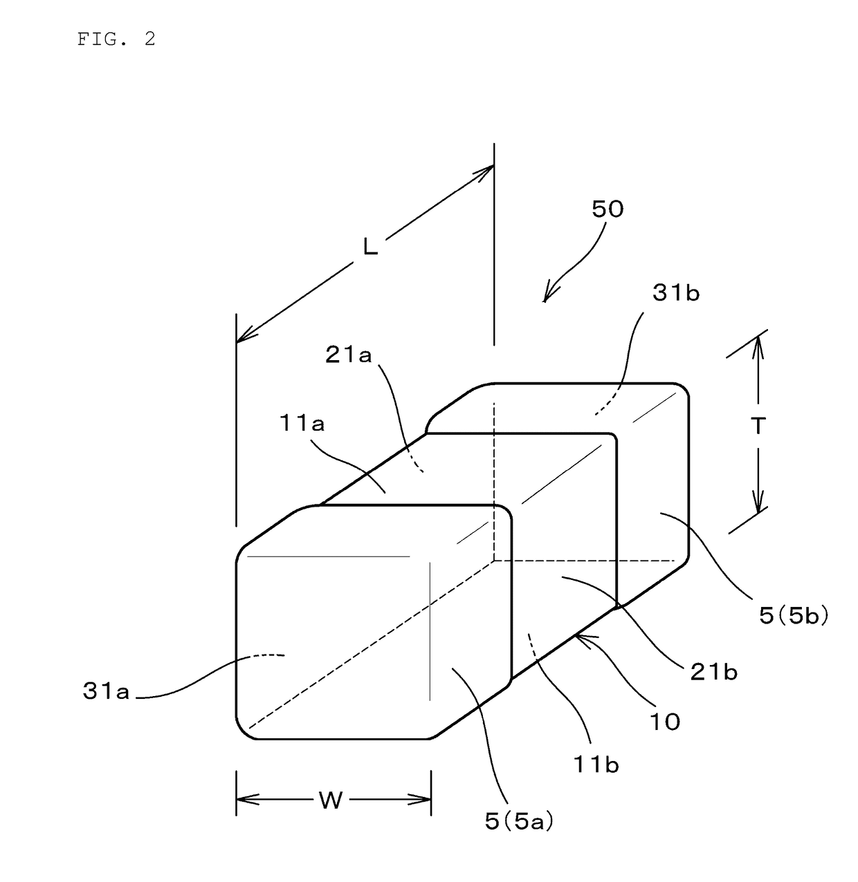
[0029]FIG. 1 is a front cross-sectional view illustrating a multilayer ceramic capacitor (electronic component) according to a preferred embodiment (First Preferred Embodiment) according to the present invention, FIG. 2 is a perspective view illustrating the multilayer ceramic capacitor in FIG. 1, and FIG. 3 is a side cross-sectional view.

[0030]The multilayer ceramic capacitor 50 preferably is provided, as shown in FIGS. 1 to 3, with an electronic component body 10 of a laminated body including dielectric layers 1 of a dielectric ceramic and multiple internal electrodes 2 (2a, 2b) provided at the multiple interfaces between the dielectric layers 1; and internal electrodes 2 (...


PUM

PropertyMeasurementUnit
thicknessaaaaaaaaaa
thicknessaaaaaaaaaa
thicknessaaaaaaaaaa

Abstract

An electronic component body includes an internal electrode that is partially extended to a surface of the electronic component body and is connected to an external electrode including a conductive material-containing resin layer including a conductive material and a resin layer and a plated layer covering the conductive material-containing resin layer. The conductive material-containing resin layer includes metal particles as the conductive material, and the plated layer extends from the surface of the conductive material-containing resin layer into the conductive material-containing resin layer such that the plated layer coats at least some of the metal particles.

Description

CROSS REFERENCE TO RELATED APPLICATIONS[0001]This application claims the benefit of priority to Japanese Patent Application 2016-149469 filed on Jul. 29, 2016 and Japanese Patent Application 2015-200893 filed on Oct. 9, 2015. The entire contents of these applications are hereby incorporated herein by reference.BACKGROUND OF THE INVENTION[0002]1. Field of the Invention[0003]The present invention relates to an electronic component, and more particularly, an electronic component including an external electrode on a surface of an electronic component body.[0004]2. Description of the Related Art[0005]In recent years, electronic components that have a structure with an external electrode formed on the surface of an electronic component body are widely used as surface-mount (chip-type) electronic components.[0006]Further, as such chip-type electronic components, JP10-284343A proposes a chip-type electronic component as described below.[0007]More specifically, JP10-284343A proposes a chip-t...

Claims


Application Information

Patent Timeline
Patent Type & Authority Applications(United States)
IPC IPC(8): H01G4/248H01G4/005H01G4/12H01G4/224H01G4/30
CPCH01G4/248H01G4/224H01G4/005H01G4/12H01G4/30H01G4/232H01G4/2325H01G4/0085H01G4/012
Inventor ZENZAI, KOTA
Owner MURATA MFG CO LTD
Why Eureka
Try Eureka