Capacitor 3d-cell and 3d-capacitor structure
- Summary
- Abstract
- Description
- Claims
- Application Information
AI Technical Summary
Benefits of technology
Problems solved by technology
Method used
Image

Examples
Embodiment Construction
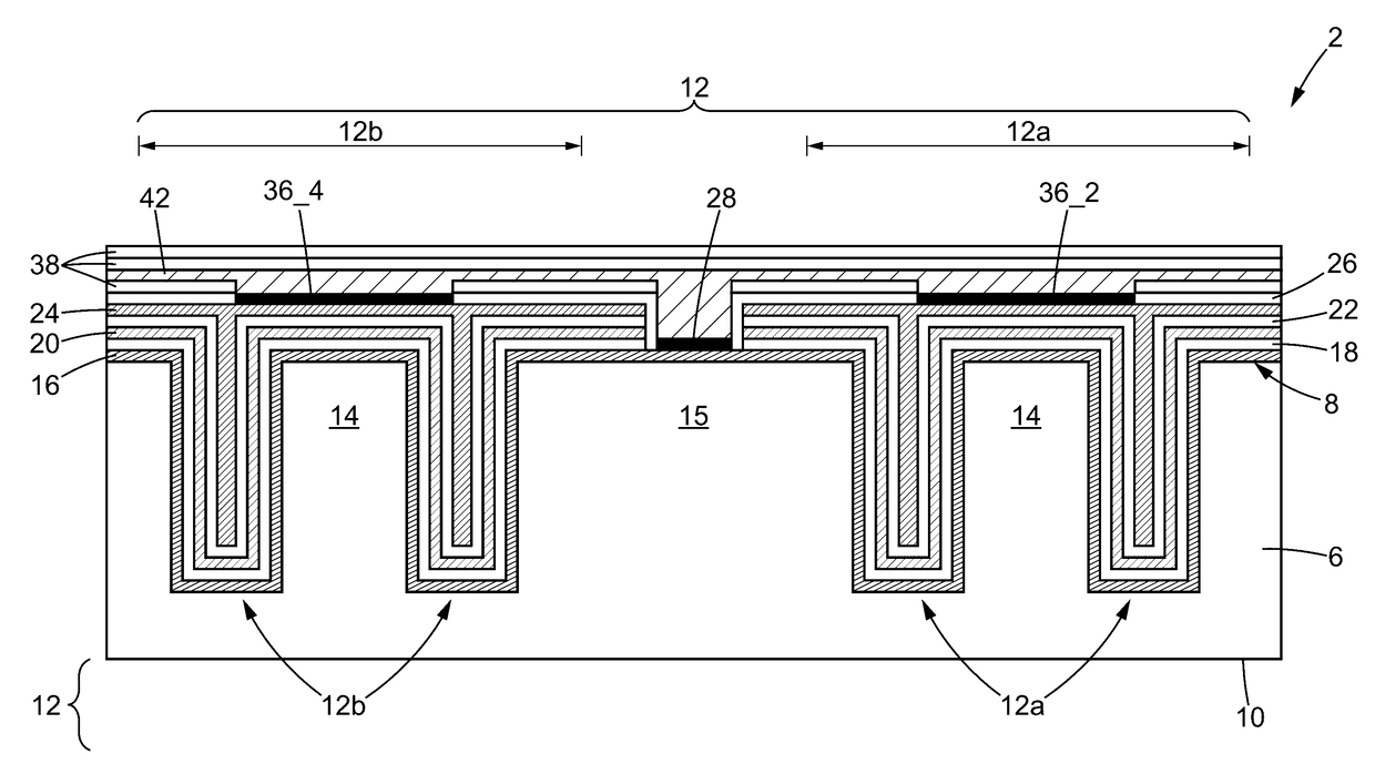
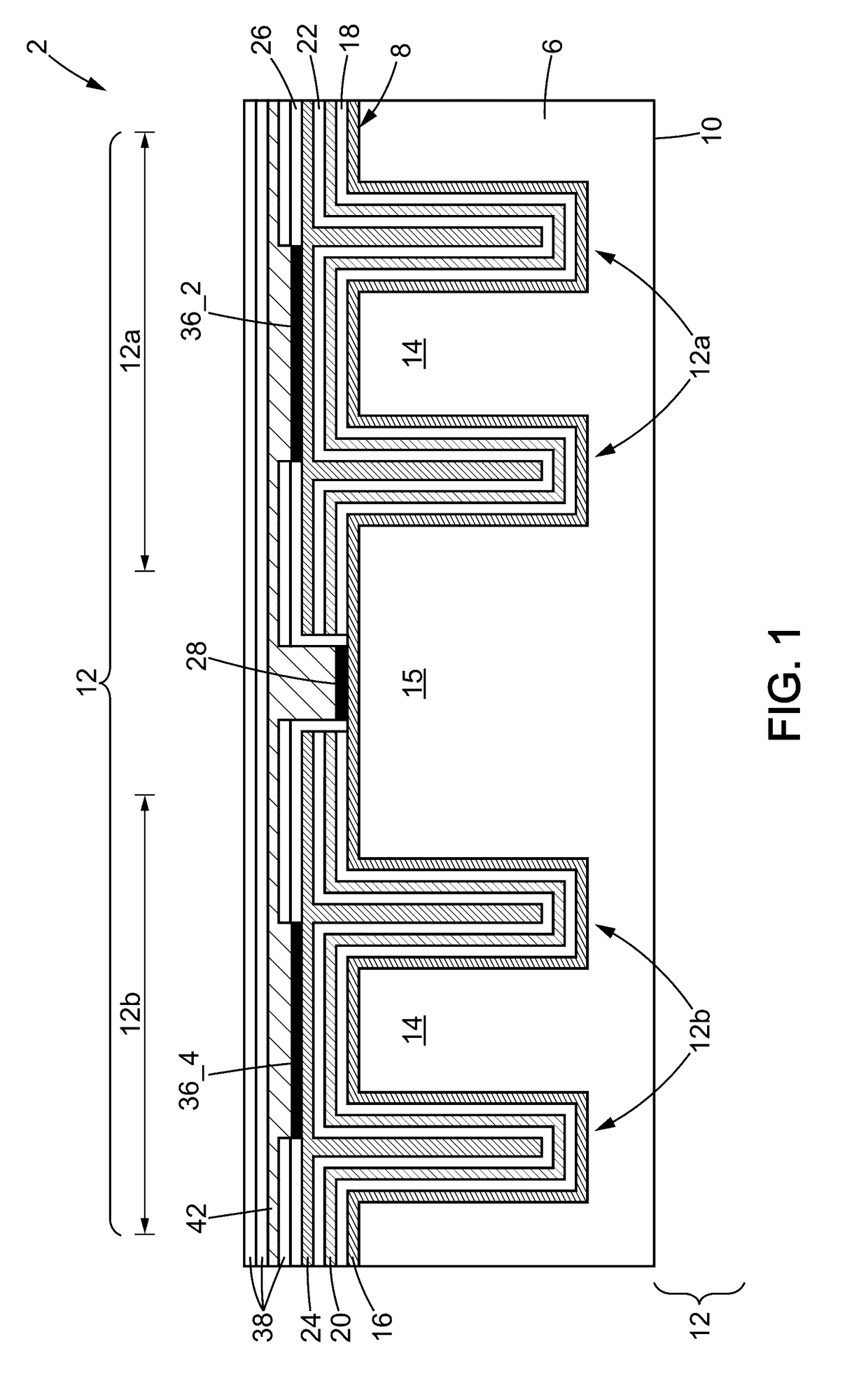
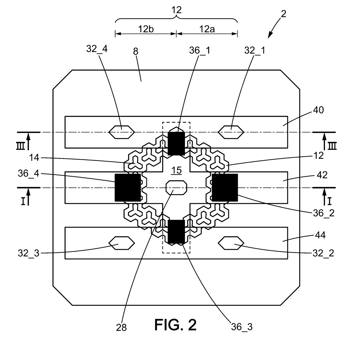
[0045]FIG. 1 shows a capacitor 3D-cell which is labelled 2 as a whole, and which may be used for forming a 3D-capacitor structure as shown in FIG. 5 and labelled 4. The capacitor structure implements a silicon substrate 6, with a top face 8 and a back face 10 which is opposite the top face 8. The thickness of the silicon substrate 6 may be adapted to adjust or increase a capacitor surface-density value of the capacitor 3D-cell 2. Part of the capacitor layers is realised in a trench 12 which is etched into the silicon substrate 6 from the top face 8. The silicon substrate 6 may be thinned down to approximately 100 μm (micrometer), but the minimum thickness of the silicon substrate 6 is determined by the depth of trench 12 which receives the capacitor layers. A crystal orientation of the silicon substrate 6 may also be selected to allow dry and / or wet etching with a desired etching direction. In the present description, the etching direction for the trench 12 is assumed to be perpendi...
PUM
 Abstract
Description
Claims
Application Information
 - Generate Ideas
- Intellectual Property
- Life Sciences
- Materials
- Tech Scout
- Unparalleled Data Quality
- Higher Quality Content
- 60% Fewer Hallucinations
Browse by: Latest US Patents, China's latest patents, Technical Efficacy Thesaurus, Application Domain, Technology Topic, Popular Technical Reports.
© 2025 PatSnap. All rights reserved.Legal|Privacy policy|Modern Slavery Act Transparency Statement|Sitemap|About US| Contact US: help@patsnap.com