Array Substrate, Display Panel and Display Device
- Summary
- Abstract
- Description
- Claims
- Application Information
AI Technical Summary
Benefits of technology
Problems solved by technology
Method used
Image

Examples
Embodiment Construction
[0031]An array substrate, a display panel and a display device provided according to embodiments of the present invention will be described in detailed in conjunction with the drawings.
[0032]In the drawings, a thickness and shape of each of the layers do not reflect a real scale of the array substrate, but are intended to schematically illustrate the content of the present invention.
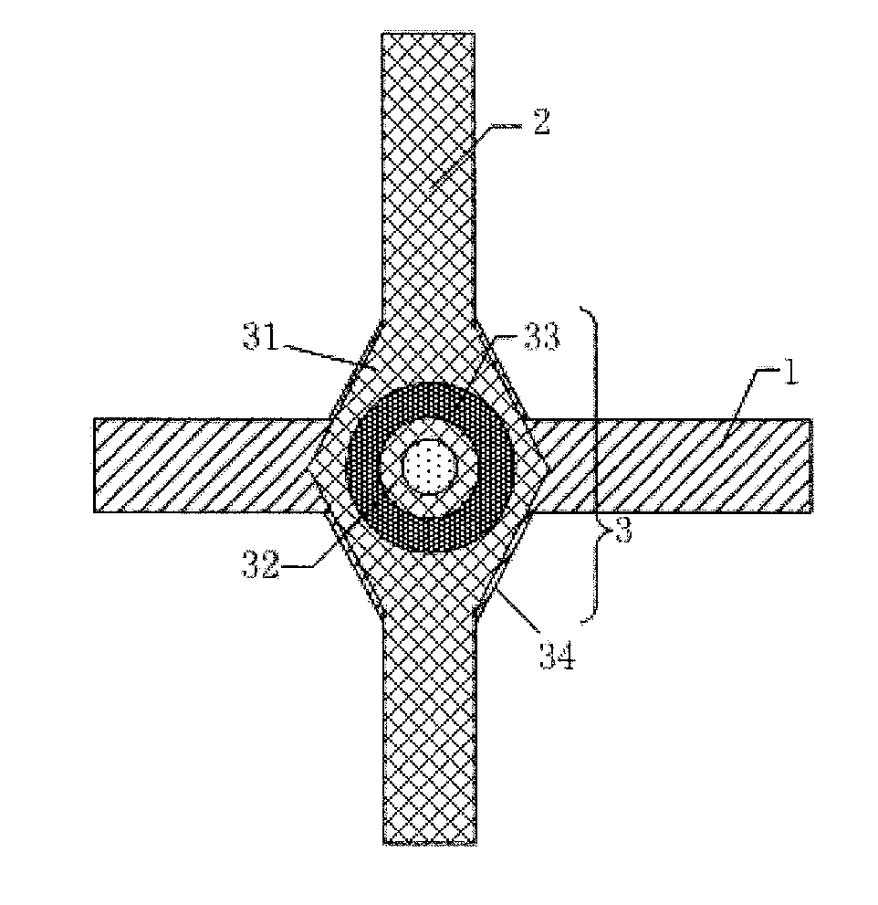
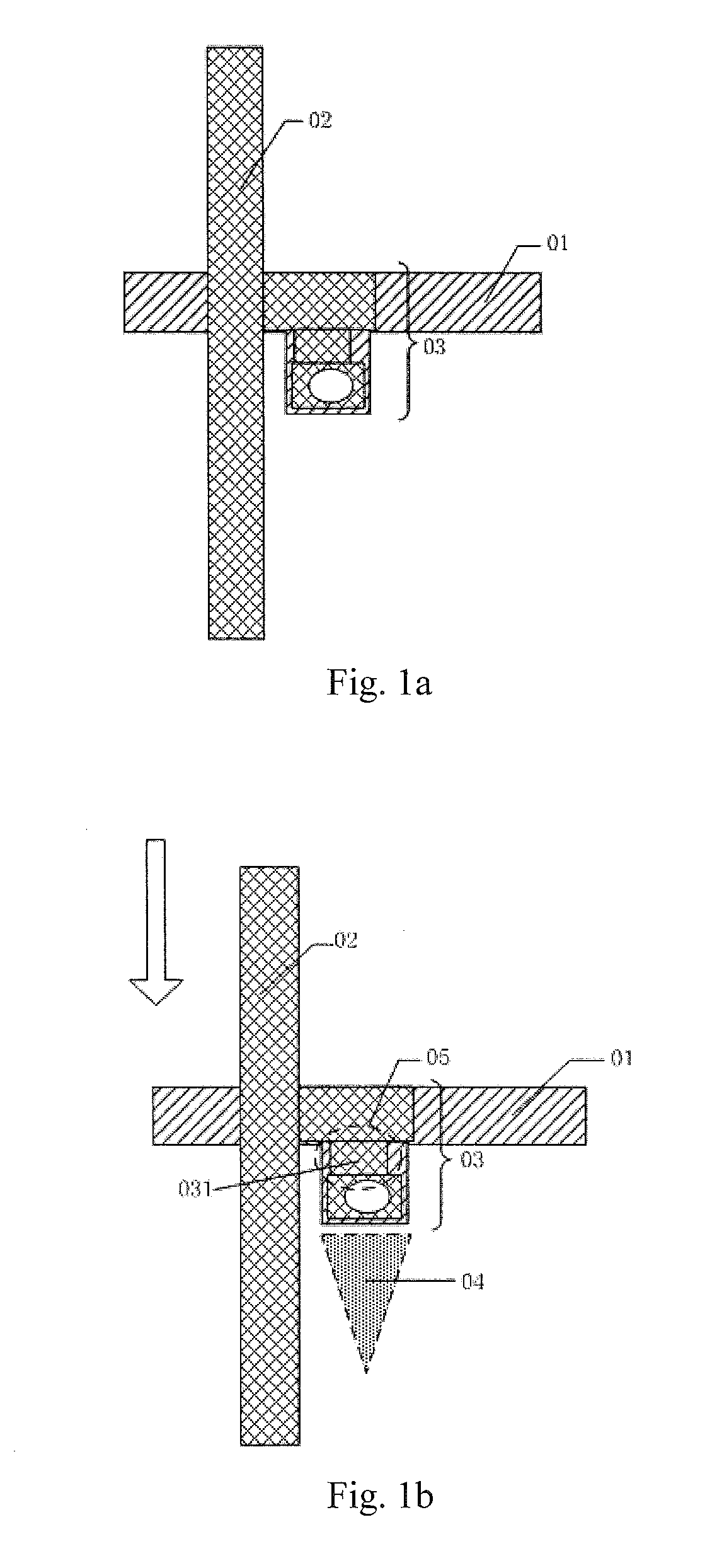
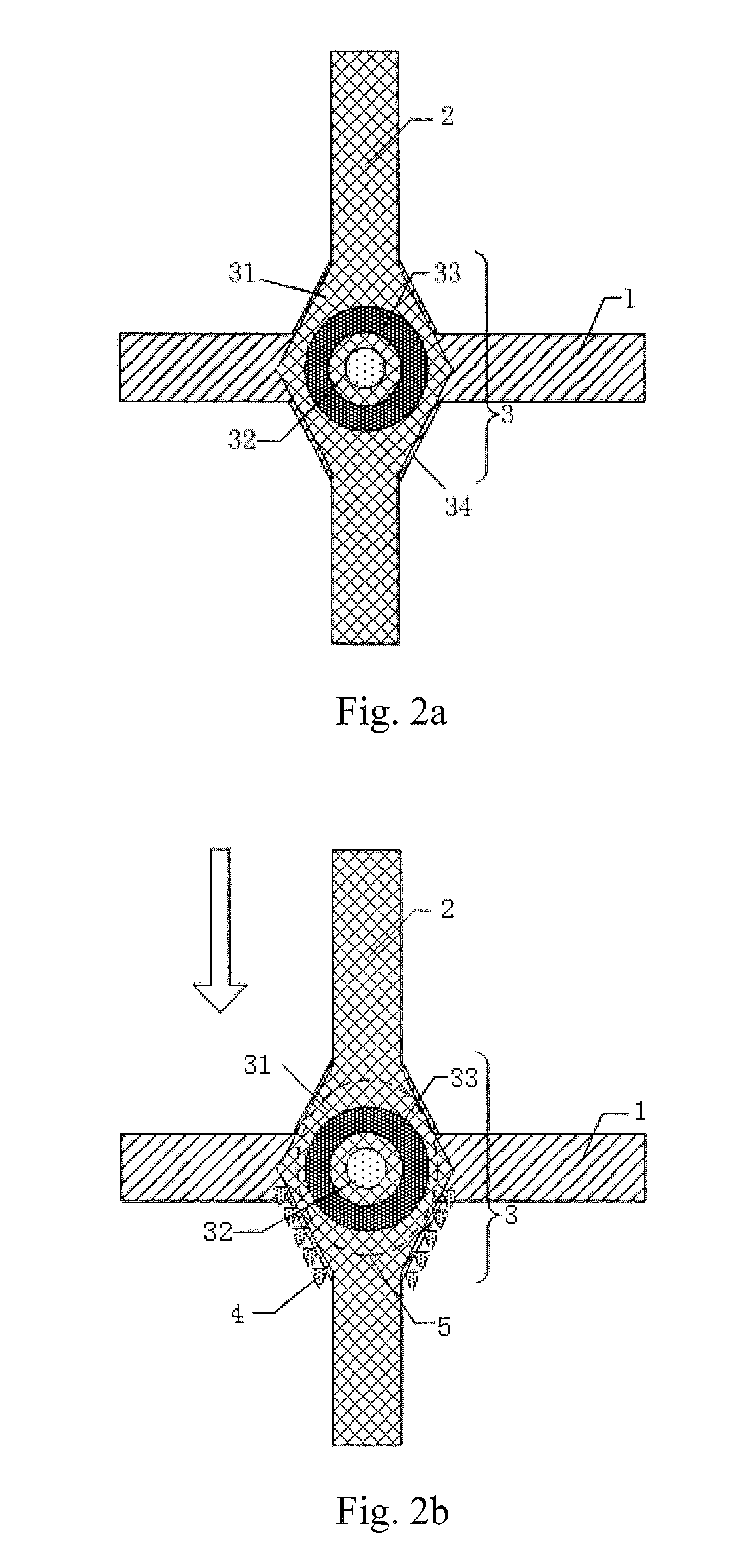
[0033]FIG. 1a illustrates a related array substrate, which includes a gate line 01 and a data line 02 which are arranged on a substrate. A thin film transistor 03 is formed at a region adjacent to a position where the gate line 01 and the data line 02 are overlapped. As shown in FIG. 1b, the thin film transistor 03 is arranged within a pixel region of the array substrate, which, on one hand, adversely affects an opening ratio of a display panel, and on the other hand, renders a rather large slightly rubbing region 04 (an arrow direction in FIG. 1b indicates a rubbing direction of an orientation film) adj...
PUM
 Abstract
Description
Claims
Application Information
 - R&D Engineer
- R&D Manager
- IP Professional
- Industry Leading Data Capabilities
- Powerful AI technology
- Patent DNA Extraction
Browse by: Latest US Patents, China's latest patents, Technical Efficacy Thesaurus, Application Domain, Technology Topic.
© 2024 PatSnap. All rights reserved.Legal|Privacy policy|Modern Slavery Act Transparency Statement|Sitemap