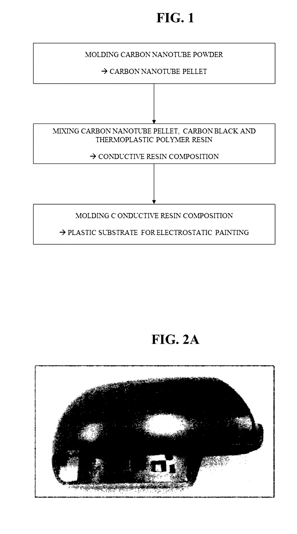
Method for manufacturing plastic substrate for electrostatic painting
a technology of electrostatic painting and plastic substrate, which is applied in the field of preparing plastic substrate for electrostatic painting, can solve the problems of economic loss and lowering the efficiency of electrostatic painting, and achieve the effects of improving economic efficiency, productivity and workability
- Summary
- Abstract
- Description
- Claims
- Application Information
AI Technical Summary
Benefits of technology
Problems solved by technology
Method used
Image
Examples
experimental example 1
Resistance According to Content Ratio of Each Component
[0071]A surface resistance of each sample prepared according to Examples 1 to 3 and Comparative Examples 1 to 4 was measured in accordance with ASTM D257, and the results are shown in the following Table 2.
TABLE 2ClassificationSurface resistance (Ω / sq)Example 11012~1013Example 2 109~1010Example 3107~108Comparative Example 1—Comparative Example 21013~1014Comparative Example 31013~1014Comparative Example 41013~1014
[0072]Referring to Table 2, a plastic substrate prepared without adding a conductive material in Comparative Example 1 has an excessively high surface resistance, so that the measurement was impossible.
[0073]Further, the surface resistances of the plastic substrates prepared in Examples 1 to 3 in which both the carbon nanotube pellet and carbon black were used was measured to be lower than those of the plastic substrate prepared in Comparative Examples 2 to 4 in which only a carbon nanotube pellet was used as a conductiv...
experimental example 2
Resistance Per Area
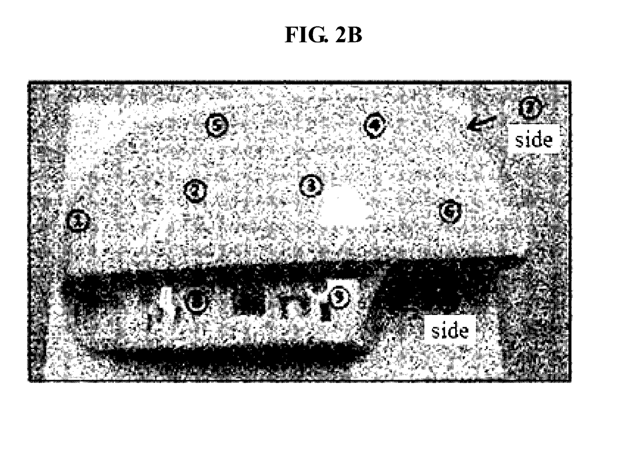
[0075]A plastic substrate for a side mirror of an automotive vehicle was prepared by extruding and injecting each of the composition of Example 3 and the thermoplastic polymer resin of Comparative Example 1 using a mold of predetermined form, and the results are shown in FIG. 2.
[0076]With respect to a plastic substrate for a side mirror of an automotive vehicle in FIG. 2A, a surface resistance of the same areas as the areas represented by the numbers in FIG. 2B was measured in accordance with ASTM D257, and the results are shown in the following Table 3.
TABLE 3AreaSurface resistance (Ω / sq) 11.1 × 10⁹ 21.3 × 10⁹ 35.0 × 10⁸ 45.2 × 10⁹ 52.3 × 10⁹ 61.1 × 10⁹ 7 (side)7.8 × 10⁸ 81.6 × 10⁹ 91.5 × 10810 (side)1.7 × 10⁹
[0077]Referring to FIG. 2A, FIG. 2B, and Table 3, in the case of a plastic substrate for electrostatic painting prepared by extrusion molding and injection molding after mixing carbon nanotube pellets and carbon black as a conductive material with a thermopl...
PUM
| Property | Measurement | Unit |
|---|---|---|
| size | aaaaa | aaaaa |
| length | aaaaa | aaaaa |
| diameter | aaaaa | aaaaa |
Abstract
Description
Claims
Application Information

