Multi-Step Atomic Layer Deposition Process for Silicon Nitride Film Formation
- Summary
- Abstract
- Description
- Claims
- Application Information
AI Technical Summary
Benefits of technology
Problems solved by technology
Method used
Image
Examples
example reactors
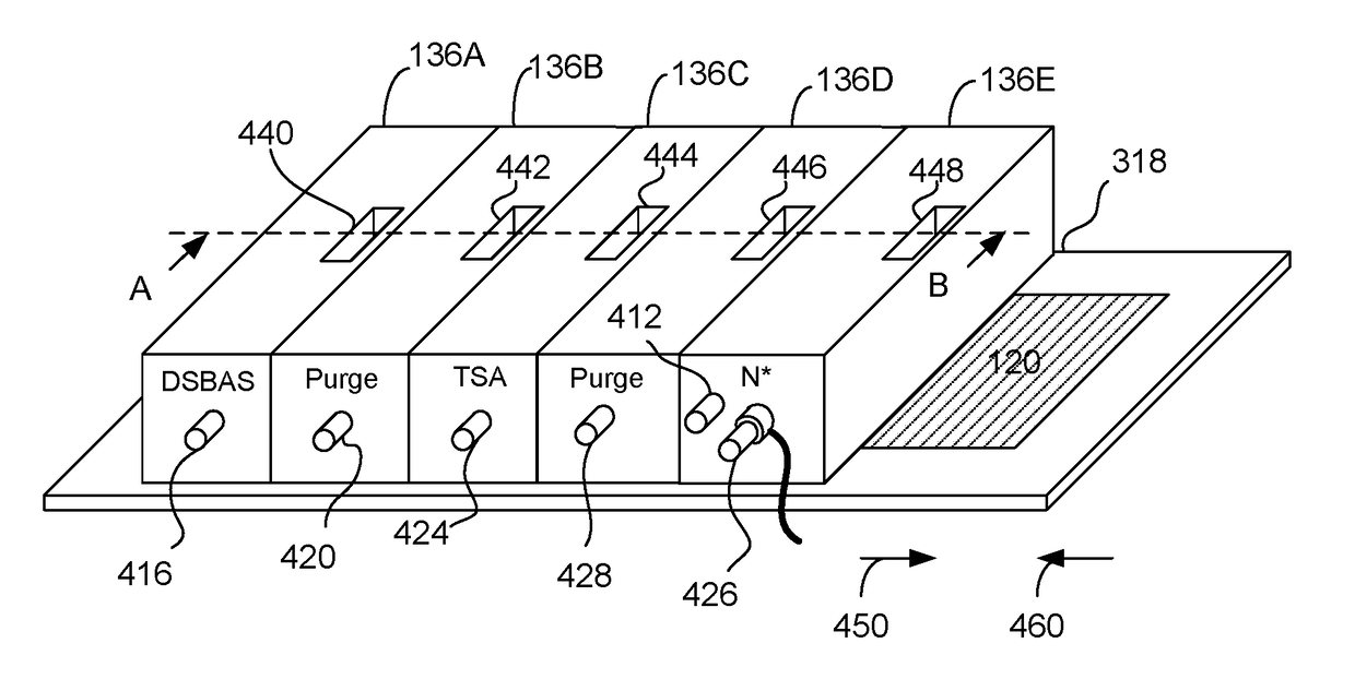
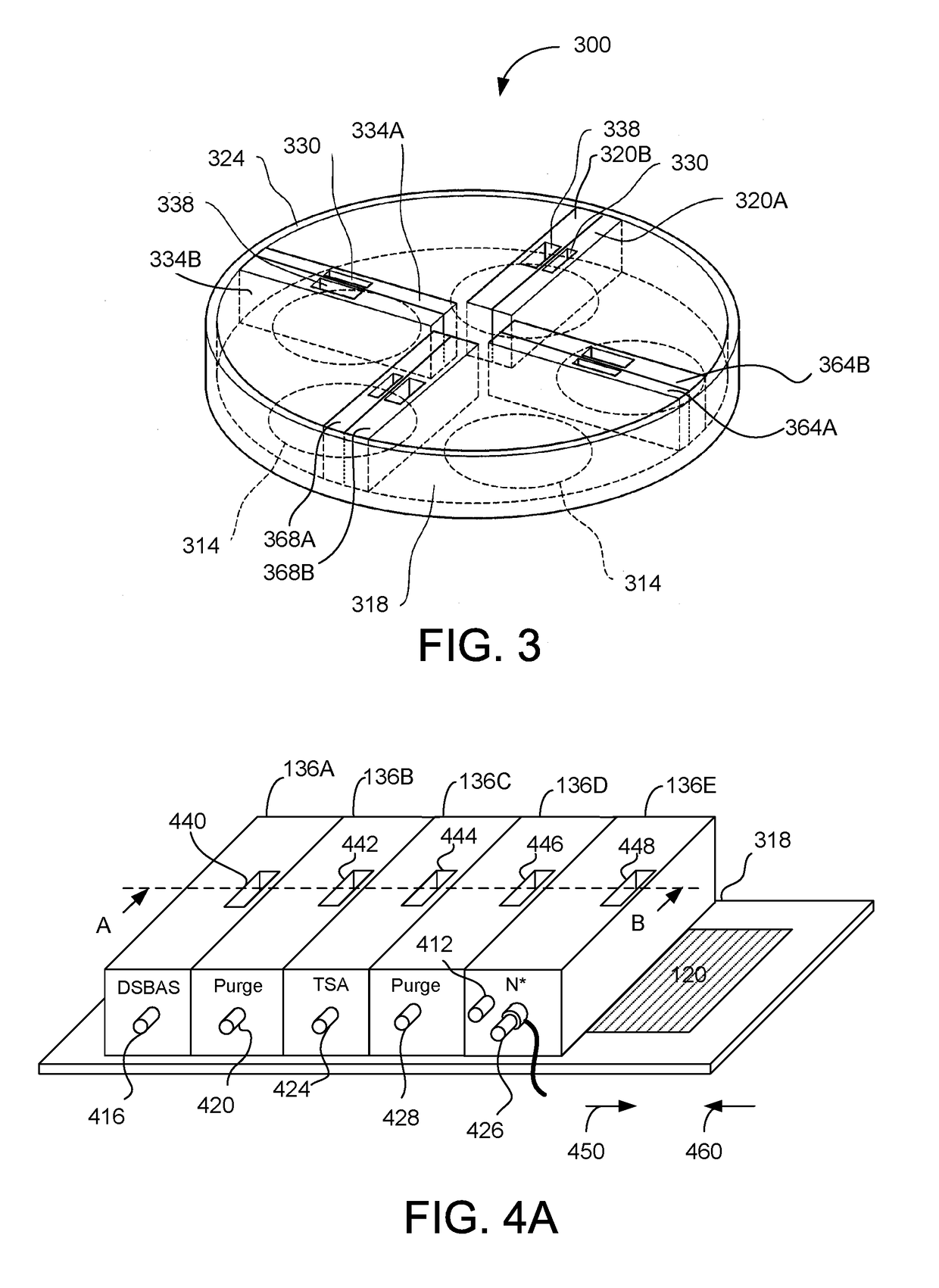
[0038]FIG. 4A is a perspective view of reactors 136A through 136E (collectively referred to herein as the “reactors 136”) in the deposition device 100 of FIG. 1, according to one embodiment. In the embodiment of FIG. 4A, the reactors 136A through 136E are placed in tandem adjacent to each other. In other embodiments, the reactors 136A through 136E may be placed at a distance from each other. As the substrate 120 moves from the left to the right (as shown by arrow 450), the substrate 120 is sequentially injected with materials by the reactors 136A through 136E to deposit a layer of material onto the substrate 120. Instead of (or in addition to) the substrate 120 being moved relative to the reactors 136, the reactors 136 may be moved relative to the substrate 120 (e.g., from right to left while injecting materials).
[0039]In one embodiment, after moving the substrate 120 from the left to the right, the substrate 120 may be moved from right to left (as shown by arrow 460) to expose the ...
PUM
| Property | Measurement | Unit |
|---|---|---|
| Thickness | aaaaa | aaaaa |
| Concentration | aaaaa | aaaaa |
| Electric potential / voltage | aaaaa | aaaaa |
Abstract
Description
Claims
Application Information


