Top-emitting organic electroluminescent display panel, manufacturing method thereof and display device

a technology of organic electroluminescent display panel and manufacturing method, applied in the field of display technology, can solve the problems of large inner stress, easy to be affected, low elasticity, etc., and achieve the effects of reducing process flow, simplifying film layer structure, and reducing the number of display panels

Active Publication Date: 2017-04-20
BOE TECH GRP CO LTD
View PDF14 Cites 4 Cited by
  • Summary
  • Abstract
  • Description
  • Claims
  • Application Information

AI Technical Summary

Benefits of technology

[0006]In view of this, the embodiments of the present invention provide a top-emitting organic electroluminescent display panel, a manufacturing method thereof, and a display device, which can simplify the film layer structure of the OLED panel, reduce the manfucturing process, shorten the light path from the light emitting layer to the color filter layer, and improve the luminous efficiency.
[0027]The embodiments of the present invention provide a top-emitting organic electroluminescent display panel, a manufacturing method thereof and a display device; the top-emitting organic electroluminescent display panel comprising: a substrate, a layer of white organic light emitting diodes and a thin film encapsulation layer arranged on the substrate in sequence; wherein the thin film encapsulation layer comprises at least two inorganic thin film layers and at least one organic thin film layer; wherein one of the at least one organic thin film layer is a color filter layer comprising filters of at least three different colors for full color display, the color filter layer being arranged between the at least two inorganic thin film layers. Since one of the organic thin film layers in the thin film encapsulation layer is a color filter layer, the color filter layer does not have to be arranged above the thin film encapsulation layer separately; in this way, it can not only reduce the film layer number of the display panel, simplify the film layer structure, reduce the process flows and reduce the manufacturing cost, but also can shorten the light path from the light emitting layer to the color filter layer, thereby improving the luminous efficiency and the display effect.

Problems solved by technology

The inorganic thin film layer 031 has a relatively high compactness and is the main water and oxygen barrier layer; however, the inorganic thin film layer 031 has a relatively low elasticity, and a large inner stress, which is easily affected by the external force so as to generate cracks or to be stripped from the OLED device.
The manufacturing process is relatively complex; moreover, the light path is increased, the luminous efficiency is reduced, and the display effect of the OLED panel is influenced.
Therefore, how to simplify the film layer structure of the OLED panel, reduce the manufacturing processes, shorten the light path, and improve the luminous efficiency is a technical problem that needs to be solved by the skilled person in the art urgently.

Method used


Image

  • Top-emitting organic electroluminescent display panel, manufacturing method thereof and display device
  • Top-emitting organic electroluminescent display panel, manufacturing method thereof and display device
  • Top-emitting organic electroluminescent display panel, manufacturing method thereof and display device

Examples


Embodiment Construction

[0032]The specific implementations of the top-emitting organic electroluminescent display panel, the manufacturing method thereof, and the display device provided by the embodiment of the present invention will be explained in detail below with reference to the drawings.

[0033]The thickness and the shape of the film layers in the drawings may not reflect the real proportion of the top-emitting organic electroluminescent display panel, but are merely for purposes of explanation and clarification of the present invention schematically.

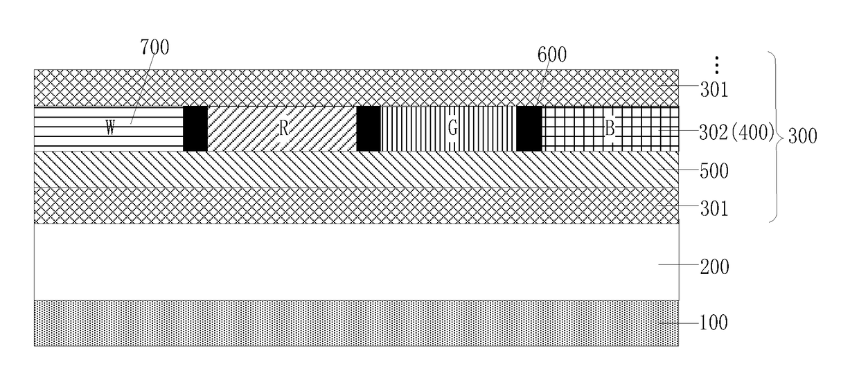
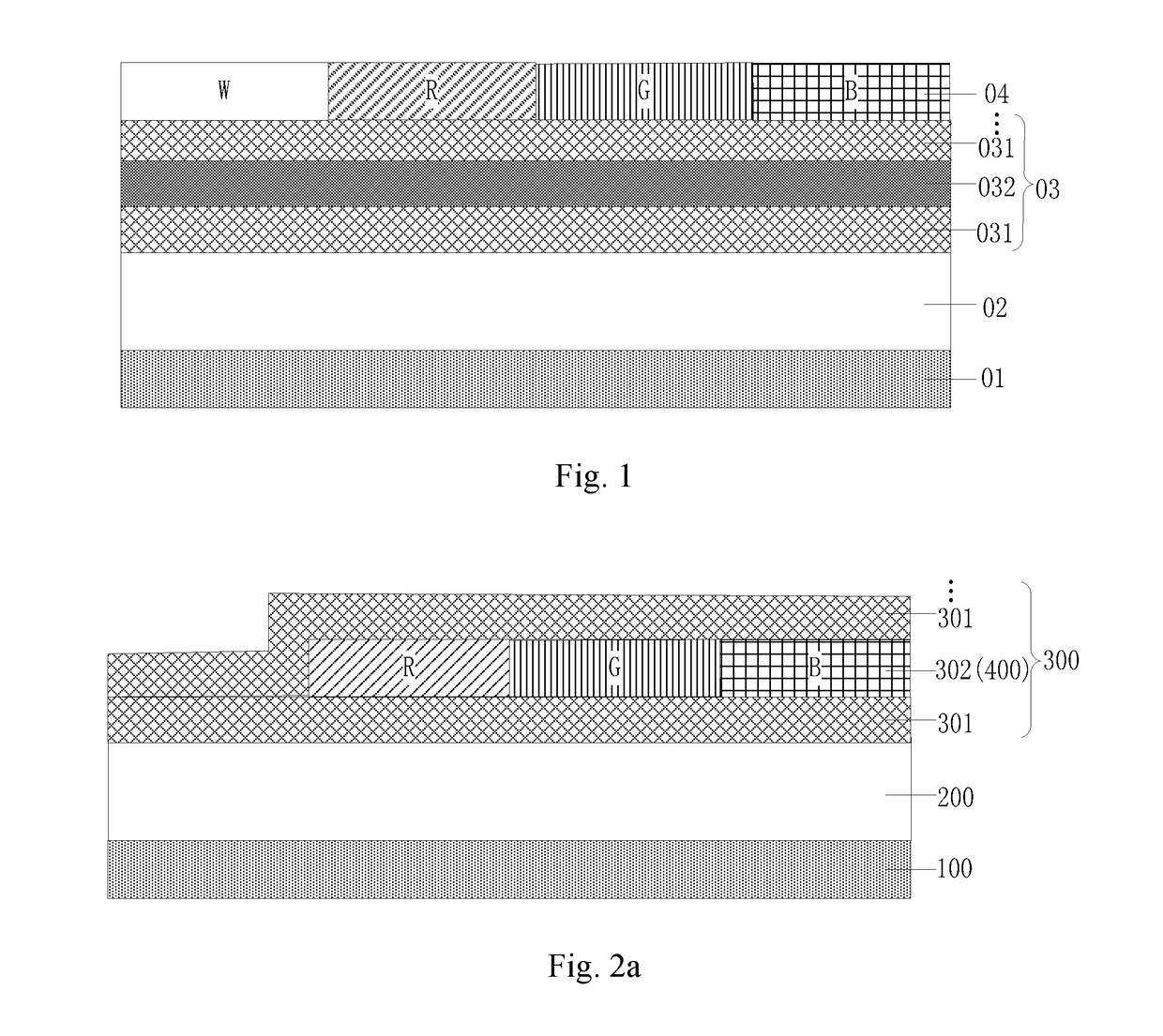
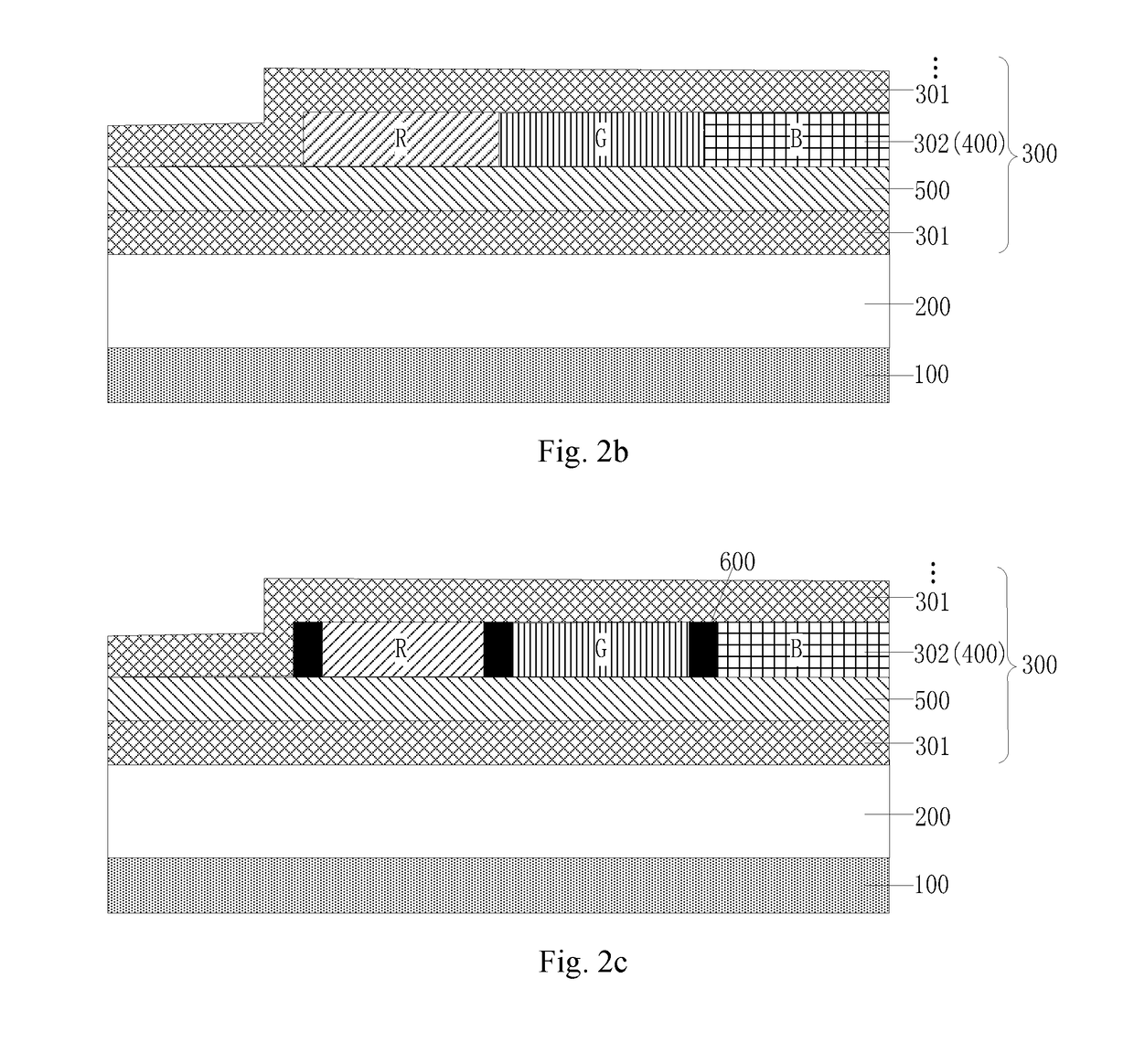
[0034]An embodiment of the present invention provides a top-emitting organic electroluminescent display panel, as shown in FIG. 2a to FIG. 2d, comprising: a substrate 100, a layer of white organic light emitting diodes 200, and a thin film encapsulation layer 300 arranged on the substrate 100 in sequence. The thin film encapsulation layer 300 comprises at least two inorganic thin film layers 301 and at least one organic thin film layer 302.

[0035]One of th...


PUM


Abstract

A top-emitting organic electroluminescent display panel, a manufacturing method, and a display device. The top-emitting organic electroluminescent display panel comprises: a substrate, a layer of white organic light emitting diodes and a thin film encapsulation layer arranged on the substrate in sequence. The thin film encapsulation layer comprises at least two inorganic thin film layers and at least one organic thin film layer. At least one organic thin film layer is a color filter layer, the color filter layer being arranged between the at least two inorganic thin film layers. Since one of the organic thin film layers in the thin film encapsulation layer is a color filter layer, the color filter layer does not have to be arranged above the thin film encapsulation layer separately, thus reducing the number of film lavers, simplifying the film layer structure, reducing manufacturing costs, and improving the luminous efficiency and the display effect.

Description

RELATED APPLICATIONS[0001]The present application is the U.S. national phase entry of PCT / CN / 2015 / 089150, with an international filing date of Sep. 8, 2015, which claims the benefit of Chinese Patent Application No. 201510104824.8, filed on Mar. 10, 2015, the entire disclosures of which are incorporated herein by reference.FIELD OF THE INVENTION[0002]The present invention relates to the field of display technology, particularly to a top-emitting organic electroluminescent display panel, a manufacturing method thereof and a display device.BACKGROUND OF THE INVENTION[0003]At present, the organic electroluminescent display and organic light emitting diode (OLED) have gradually become the mainstream of the display field due to their excellent performance of low power consumption, high color saturation, wide visual angle, small thickness, and flexibility. The OLED can be classified into bottom-emitting type and top-emitting type according to the light emission manner. The light emission ...

Claims


Application Information

Patent Timeline
Patent Type & Authority Applications(United States)
IPC IPC(8): H01L27/32H01L51/56H01L51/52
CPCH01L27/322H01L51/56H01L51/5284H01L51/5253H10K59/38H10K50/865H10K50/844H10K71/00
Inventor LEE, JOOHYEONHUANGFU, LUJIANGPARK, JINSAN
Owner BOE TECH GRP CO LTD
Why Eureka
Try Eureka