Display device with separation member including steps

a technology of separation member and display device, which is applied in the direction of semiconductor devices, basic electric elements, electrical appliances, etc., can solve the problems of difficult to ensure sufficient alignment accuracy, difficult to perform correct image display corresponding to inputted image signals, and difficulty in filling each emission region with a predetermined organic layer with reliability. , to achieve the effect of increasing the numerical aperture and preventing a leakage current from occurring

Active Publication Date: 2017-04-20
SONY CORP
View PDF0 Cites 3 Cited by
  • Summary
  • Abstract
  • Description
  • Claims
  • Application Information

AI Technical Summary

Benefits of technology

[0010]However, it is expected that a further increase in the numerical aperture will be demanded in future. Therefor

Problems solved by technology

For this reason, it is expected in future that if the above-mentioned interval is further reduced, it will be difficult to fill each emission region with a predetermined organic layer sufficiently with reliability.
This is because there is such a concern that it might be difficult to ensure sufficient accuracy of alignment between the opening of the insulating layer and the opening of the shadow mask, or

Method used


Image

  • Display device with separation member including steps
  • Display device with separation member including steps
  • Display device with separation member including steps

Examples


Embodiment Construction

[0033]An embodiment of the present disclosure (hereinafter merely referred to as the embodiment) will be described below in detail with reference to the drawings.

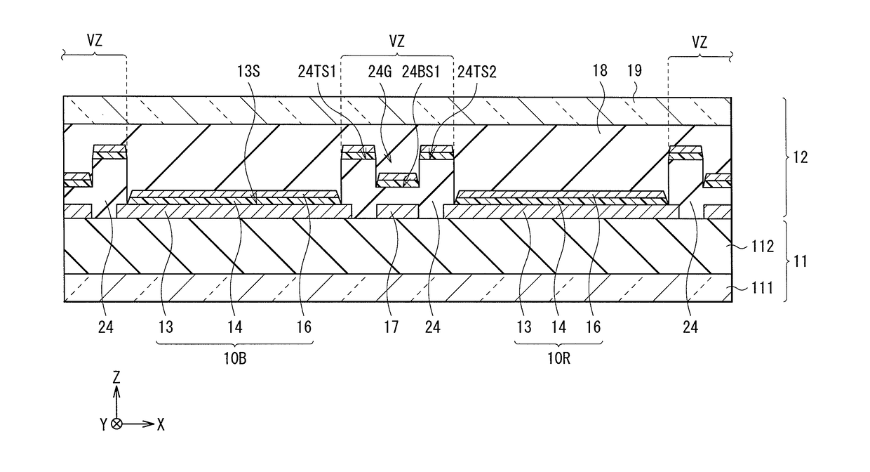
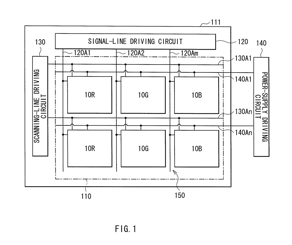
[0034]FIG. 1 illustrates a configuration of a display device using an organic light-emission element according to an embodiment in the present disclosure. This display device is used as an extra-thin organic light-emitting color display device or the like. In this display device, a display region 110 is formed on a board 111. Around the display region 110 on the board 111, a signal-line driving circuit 120 that is a driver for image display, a scanning-line driving circuit 130, and a power-supply-line driving circuit 140 are formed, for example.

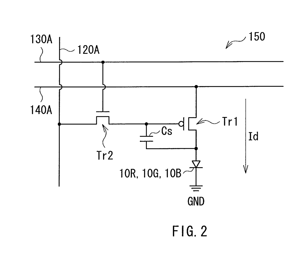
[0035]Formed in the display region 110 are a plurality of organic light-emission elements 10 (10R, 10G, and 10B) two-dimensionally arranged in the form of a matrix, and a pixel driving circuit 150 for driving the organic light-emission elements. In the pixel driving circuit 150, a pl...


PUM


Abstract

A display device includes: a substrate; a plurality of light-emission elements arranged, on the substrate, in a first direction and a second direction intersecting each other, each of the light-emission elements having a first electrode layer, an organic layer including a luminous layer, and a second electrode layer which are laminated in that order; and a separation section disposed, on the substrate, between the light-emission elements adjacent to each other in the first direction, the separation section having two or more pairs of steps. The first electrode layers in the light-emission elements are separated from each other, and the organic layers as well as the second electrode layers in the light-emission elements adjacent to each other in the first direction are separated from each other by the steps included in the separation section.

Description

RELATED APPLICATIONS[0001]This application is continuation of and claims the benefit under 35 U.S.C. §120 of U.S. patent application Ser. No. 15 / 095,272, titled “DISPLAY DEVICE WITH SEPARATION MEMBER INCLUDING STEPS,” filed on Apr. 11, 2016 which is continuation of and claims the benefit under 35 U.S.C. §120 of U.S. patent application Ser. No. 14 / 579,088 titled “DISPLAY DEVICE WITH SEPARATION MEMBER INCLUDING STEPS,” filed on Dec. 22, 2014, now U.S. Pat. No. 9,312,318, which claims the benefit under 35 U.S.C. §120 of U.S. patent application Ser. No. 14 / 302,345 titled “METHOD OF FABRICATING A DISPLAY DEVICE WITH STEP CONFIGURATION IN THE INSULATING LAYER,” filed on Jun. 11, 2014, now U.S. Pat. No. 8,956,899, which claims the benefit under 35 U.S.C. §120 as a divisional application of U.S. patent application Ser. No. 13 / 206,762, titled “DISPLAY DEVICE WITH STEP CONFIGURATION IN THE INSULATING LAYER,” filed Aug. 10, 2011, now U.S. Pat. No. 8,772,797, which claims priority to Japanese P...

Claims


Application Information

Patent Timeline
IPC IPC(8): H01L27/32H01L51/50H01L51/56H01L51/52
CPCH01L27/3246H01L27/3276H01L51/5206H01L2227/323H01L51/5228H01L51/56H01L51/5012H01L2924/0002H10K59/35H10K59/122H01L2924/00H01L27/1463H01L33/60H01L33/505H01L33/502H01L31/02327H01L33/36H01L33/08H10K50/11H10K50/81H10K50/824H10K59/124H10K59/131H10K59/352H10K71/00H10K50/125H10K59/123H10K59/1201H01L25/0753H01L27/156H01L33/44H01L25/0756
Inventor SAGAWA, HIROSHI
Owner SONY CORP
Why Eureka
Try Eureka