

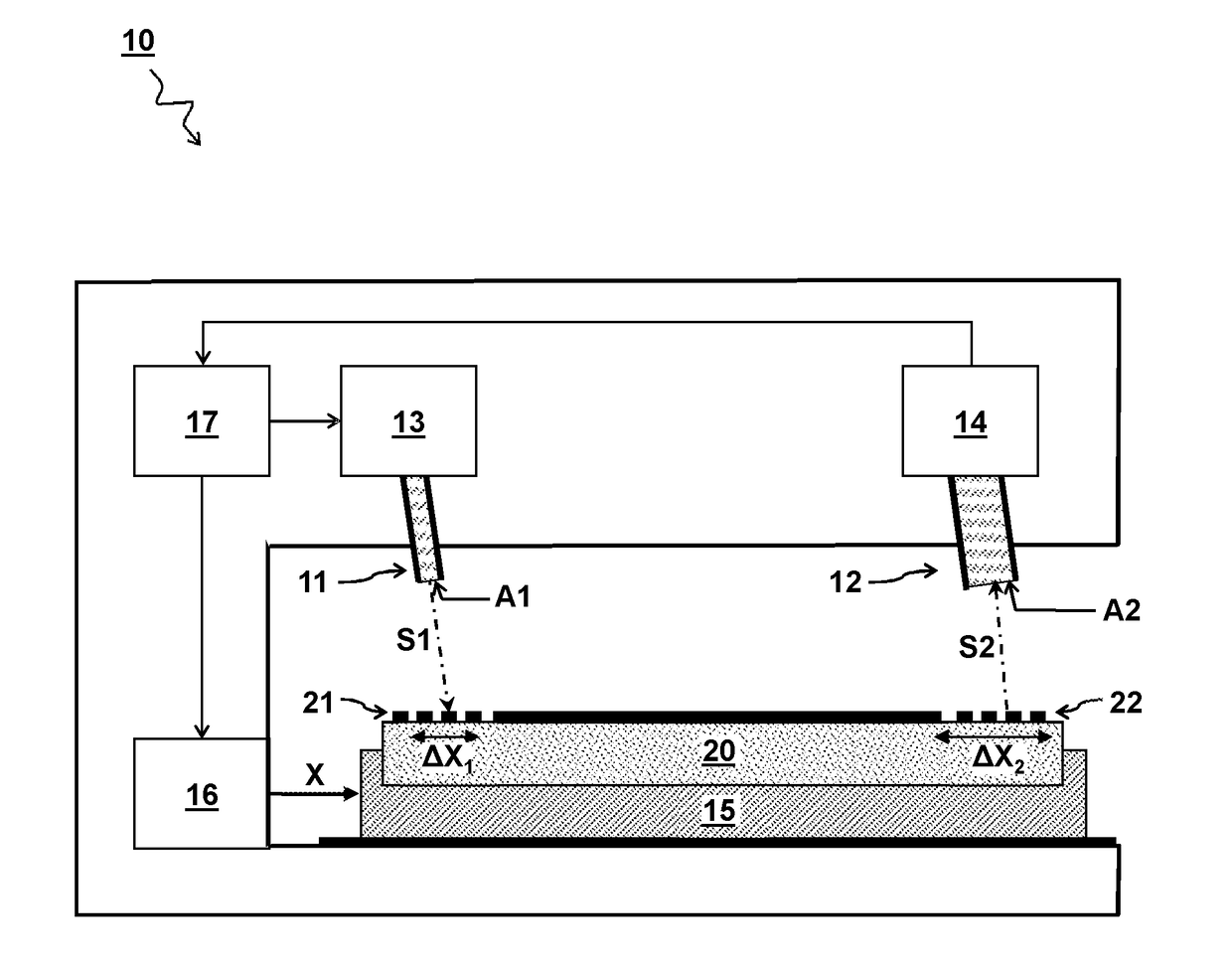
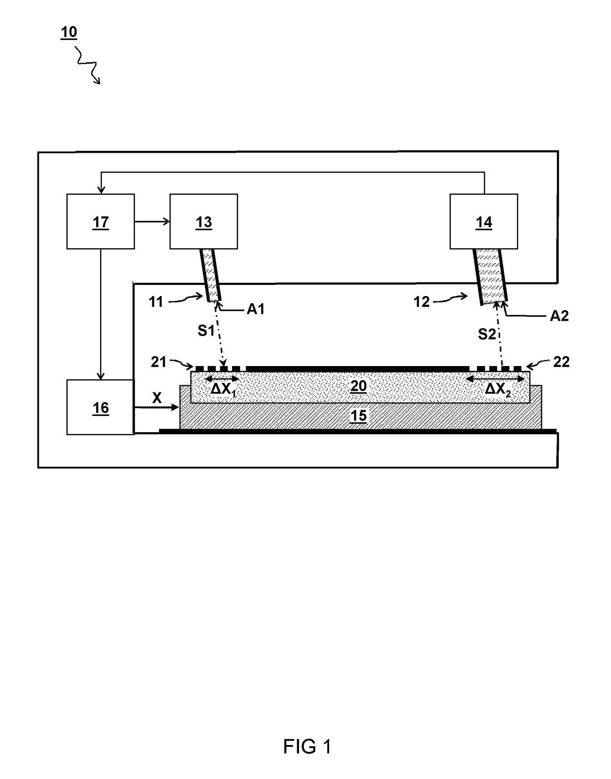
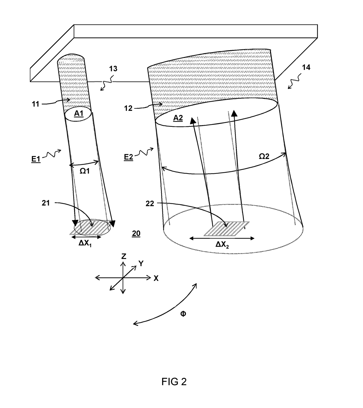
Apparatus and method for reading out an optical chip
a technology of optical chips and apparatus, applied in the field of apparatus and methods for reading out optical chips, can solve the problems of affecting the performance of optical chips, so as to avoid the possibility of damaging the contact between the optical chip and the emitter/receiver surface, reduce the cost of permanent connection, and increase the distance
- Summary
- Abstract
- Description
- Claims
- Application Information
AI Technical Summary
Benefits of technology
Problems solved by technology
Method used
Image

Examples
Embodiment Construction
[0035]Unless otherwise defined, all terms (including technical and scientific terms) used herein have the same meaning as commonly understood by one of ordinary skill in the art to which this invention belongs as read in the context of the description and drawings. It will be further understood that terms, such as those defined in commonly used dictionaries, should be interpreted as having a meaning that is consistent with their meaning in the context of the relevant art and will not be interpreted in an idealized or overly formal sense unless expressly so defined herein. In some instances, detailed descriptions of well-known devices and methods may be omitted so as not to obscure the description of the present systems and methods. Terminology used for describing particular embodiments is not intended to be limiting of the invention. As used herein, the singular forms “a”, “an” and “the” are intended to include the plural forms as well, unless the context clearly indicates otherwise...
PUM
 Abstract
Description
Claims
Application Information