Display substrate, method of manufacturing the same, display panel and display device

a technology of display substrate and substrate, applied in non-linear optics, instruments, optics, etc., can solve the problems of residual image, slow discharge, and increase the delay of signal during the transmission process, so as to reduce the driving voltage needed for pixel display, reduce power consumption, and reduce storage capacitance

Active Publication Date: 2017-05-11
BOE TECH GRP CO LTD
View PDF4 Cites 1 Cited by
  • Summary
  • Abstract
  • Description
  • Claims
  • Application Information

AI Technical Summary

Benefits of technology

[0025]As for the display substrate provided by the present disclosure, the distance between the projection of the second electrode thereof and the gap between the adjacent first electrodes is smaller than the thickness of the insulating layer between the first electrodes and the second electrode. Compared to known devices, the distance between the gap between the adjacent first electrodes and the region on the second electrode corresponding to the gap is smaller so as to reduce the storage capacitance among the first electrodes and second electrode in case where the thickness of the insulating layer between the first electrodes and second electrode is great. This configuration avoids problems such as display errors, residual images, and display green shift. Driving voltage needed by pixel display is reduced, and thus power consumption is reduced.
[0026]The method of manufacturing the display substrate provided by the present disclosure prepares the display substrate which may reduce the storage capacitance among the first electrodes and second electrode in case where the thickness of the insulating layer between the first electrodes and second electrode is great. This configuration avoids problems such as display errors, residual images, and display green shift. Driving voltage needed by pixel display is reduced, and thus power consumption is reduced.
[0027]The display panel provided by the present disclosure may be used to reduce the storage capacitance among the first electrodes and second electrode in case where the thickness of the insulating layer between the first electrodes and second electrode is great. This configuration avoids problems such as display errors, residual images, and display green shift. Driving voltage needed by pixel display is reduced, and thus power consumption is reduced.
[0028]The display device provided by the present disclosure may be used to reduce the storage capacitance among the first electrodes and second electrode in case where the thickness of the insulating layer between the first electrodes and second electrode is great. This configuration avoids problems such as display errors, residual images, and display green shift. Driving voltage needed by pixel display is reduced, and thus power consumption is reduced.

Problems solved by technology

However, along with increase of size and improvement of resolution, the delay of signal during a transmission process increases.
Moreover, storage capacitance between common electrode and pixel electrode will also become overlarge, which will lead to problems such as display errors in row direction, slow discharge, and residual image etc.
However, the solution above creates a problem.
As shown in FIG. 2, when the thickness of the insulating layer 13 between the common electrode 12 and the pixel electrode 14 increases, driving voltage of the display device will also increase, which may result in an increase of power consumption of the display device.

Method used


Image

  • Display substrate, method of manufacturing the same, display panel and display device
  • Display substrate, method of manufacturing the same, display panel and display device
  • Display substrate, method of manufacturing the same, display panel and display device

Examples


Embodiment Construction

[0040]Preferred embodiments of the present disclosure will be specified in detail in conjunction with drawings below. It shall be appreciated that the preferred embodiments described here are only used to described and explain the present disclosure, but will not be used to restrict the present disclosure.

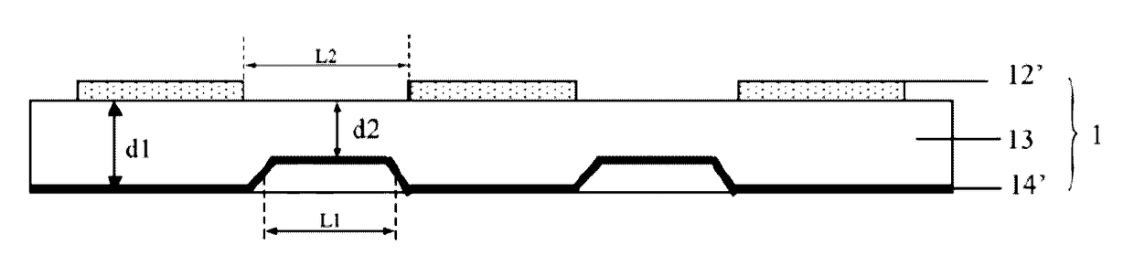
[0041]The present disclosure provides an embodiment of a display substrate. FIG. 3 is a schematic diagram of the display substrate provided by an embodiment of the present disclosure. As shown in FIG. 3, in this embodiment, the display substrate 1 is an ADS display substrate, including a first electrode 12′ and a second electrode 14′, and an insulating layer 13 arranged between the first electrode 12′ and second electrode 14′, wherein the first electrode 12′ is positioned above the second electrode 14′. The first electrode 12′ is preferably a bar-shaped electrode, and the second electrode 14′ is preferably a plane-shaped electrode. The second electrode 14′ includes a plurality of p...


PUM

PropertyMeasurementUnit
widthaaaaaaaaaa
heightaaaaaaaaaa
thicknessaaaaaaaaaa

Abstract

The present disclosure provides a display substrate including a plurality of first electrodes, a second electrode, and an insulating layer arranged among the first electrodes and the second electrode. The first electrodes are positioned above the second electrode. The second electrode includes a plurality of projections each, corresponding to a gap between two adjacent first electrodes and projecting towards the first electrodes.

Description

CROSS-REFERENCE TO RELATED APPLICATION[0001]The present disclosure is a National Stage entry of PCT / CN2015 / 091965 filed Oct. 15, 2015, which claims the benefit and priority of Chinese patent application No. 201510335054.8 filed on Jun. 16, 2015, both of which are incorporated herein by reference in their entirety.BACKGROUND[0002]The embodiments of the present disclosure relate to the display technical field, and particularly relate to a display substrate, a method of manufacturing the same, a display panel, and a display device.[0003]A display device in mode of Advanced Super Dimension Switch (hereinafter referred to as ADS), by means of an electric field generated at edge of slit electrodes disposed within the same plane and a multi-dimensional electric field formed between the slit electrode layer and a plane-shaped electrode layer, enables all the liquid crystal molecules in a liquid crystal layer located between and above the slit electrodes to rotate and increase transmittance ...

Claims


Application Information

Patent Timeline
Patent Type & Authority Applications(United States)
IPC IPC(8): G02F1/1343G02F1/1333
CPCG02F1/134309G02F1/133345G02F2201/121G02F2201/123G02F1/13439G02F1/134363G02F1/134372
Inventor WANG, YINGTAO
Owner BOE TECH GRP CO LTD
Why Eureka
Try Eureka