PWM modulation assembly of H-bridge drive circuit

A bridge driving circuit and driving circuit technology, applied in the field of PWM modulation components, can solve problems such as negative pressure at the first output terminal, and achieve the effect of facilitating adjustment, reducing current capacity, and reducing storage capacitance.

Pending Publication Date: 2020-08-04
SHANGHAI ORIENT CHIP TECH CO LTD +1
View PDF0 Cites 0 Cited by
  • Summary
  • Abstract
  • Description
  • Claims
  • Application Information

AI Technical Summary

Problems solved by technology

However, since it takes time to turn on the device, in order to prevent the through current, after the upper left transistor M1 is turned off, the left lower transistor M3 is turned on. During this switching period, the inductor current will briefly return to the load through the body diodes of the right lower transistor M4 and the left lower transistor M3. Inductor L1, resulting in a negative voltage at the first output DO
[0005] In order to solve the above three shortcomings of the NMOS tube used on the H-bridge and the negative pressure problem generated by the H-bridge during PWM speed regulation, it is necessary to design a new type of PWM modulation component for the H-bridge drive circuit

Method used


Image

  • PWM modulation assembly of H-bridge drive circuit
  • PWM modulation assembly of H-bridge drive circuit
  • PWM modulation assembly of H-bridge drive circuit

Examples


Embodiment Construction

[0030] Below in conjunction with the drawings, preferred embodiments of the present invention are given and described in detail.

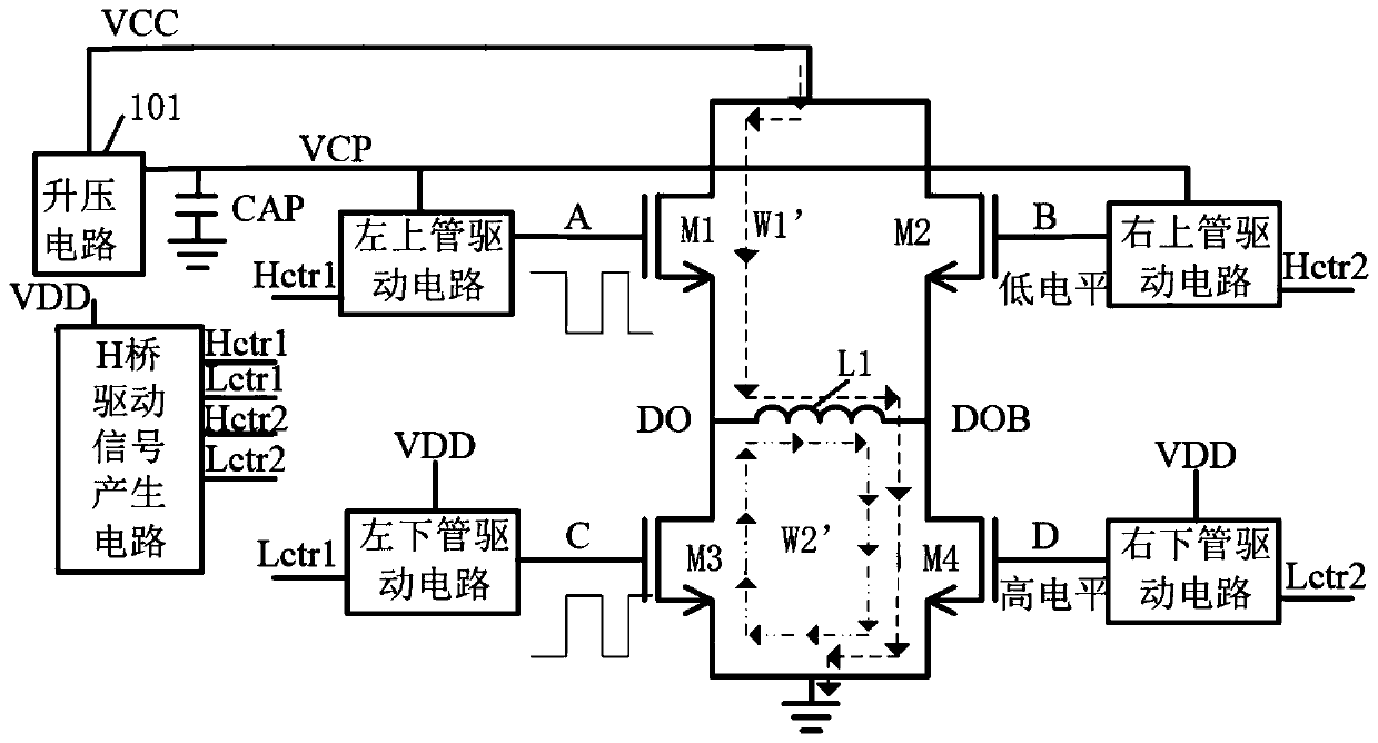
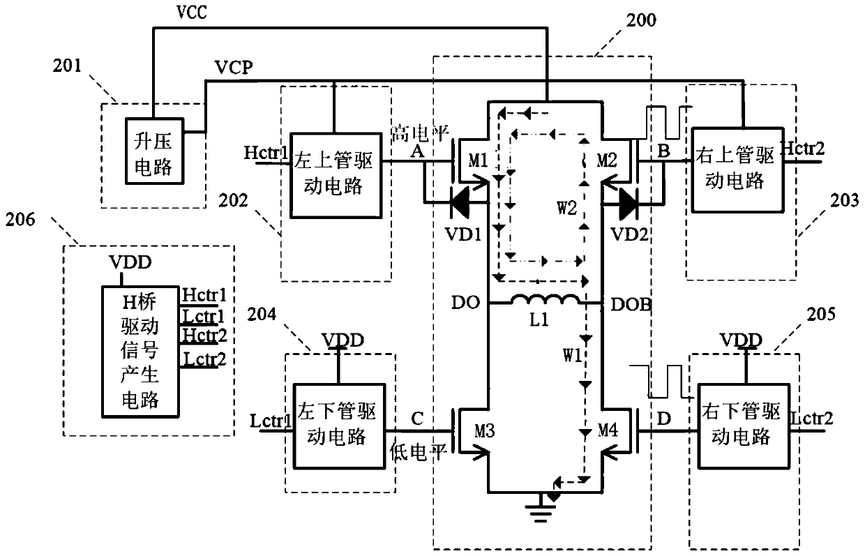
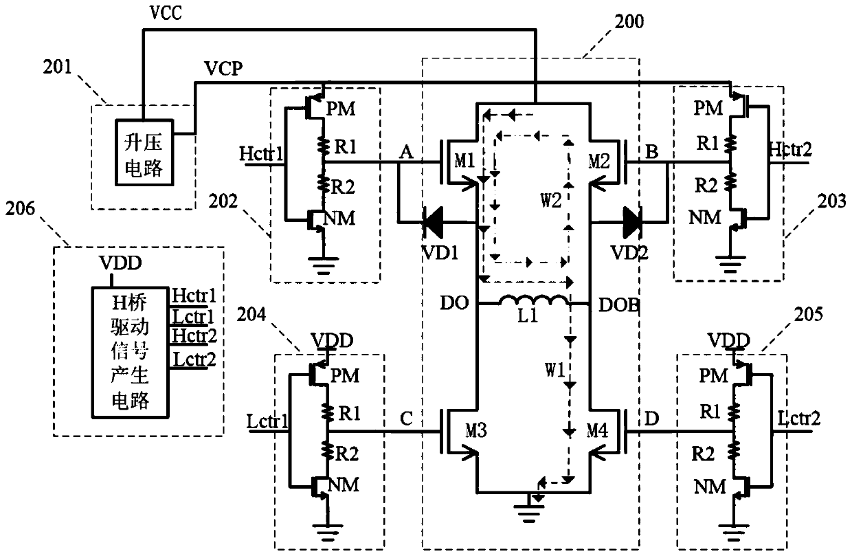
[0031] Such as Figure 2-Figure 3 Shown is the PWM modulation component of the H-bridge drive circuit according to an embodiment of the present invention, which includes a chip H-bridge drive circuit 200, and the four switch tubes of the H-bridge drive circuit 200 are all NMOS tubes, including For the left upper tube M1 and left lower tube M3 and the right upper tube M2 and right lower tube M4, in this embodiment, the left side is defined as the first side, and the right side is defined as the second side. The drains of the upper left tube M1 and the upper right tube M2 are all connected to the power supply voltage VCC of a chip, the sources of the lower left tube M3 and the lower right tube M4 are all grounded, and the H bridge driving circuit 200 is on the left side (the source of the upper left tube M1 pole and the drain of the lower left trans...


PUM


Abstract

The invention provides a PWM modulation assembly of an H-bridge drive circuit. Four switch tubes of the H-bridge drive circuit are NMOS tubes. Gates of the switch tubes are respectively connected withthe drive circuit; the input end of the drive circuit is connected with the signal output end of an H-bridge drive signal generation circuit; the H-bridge drive signal generation circuit continuouslyoutputs a conduction signal to the drive circuit corresponding to an upper tube on one side, continuously outputs a cut-off signal to the drive circuit corresponding to a lower tube on the other side, and alternately outputs cut-off and conduction signals to the drive circuits corresponding to an upper tube and a lower tube on the other side. According to the modulation assembly, the upper tube on the first side is always in a conduction state, and large parasitic capacitance exists between the grid electrode of the upper tube on the first side and the power supply voltage, so that the storage capacitance of a boost circuit is greatly reduced; and the upper tube on the first side is conducted, and the lower tube on the first side is cut off, so that the output end of the H-bridge drive circuit cannot generate negative voltage, and the circuit works more reliably than before.

Description

technical field [0001] The invention relates to an H bridge drive circuit, in particular to a PWM modulation component of the H bridge drive circuit. Background technique [0002] Integrated H-bridge driver chips are widely used in DC brushless motors. In the traditional H-bridge drive circuit designed with integrated circuit technology, the upper tube of the H-bridge generally uses a PMOS tube, and the lower tube of the H-bridge generally uses an NMOS tube. When the withstand voltage and area are equal, the on-resistance of the PMOS transistor is much larger than that of the NMOS transistor. In applications where the driving current is large and the on-resistance is required to be small, using a PMOS tube as the upper tube of the H-bridge requires a very large area to achieve a small on-resistance, which makes the chip cost high and packaging difficult. This leads to the fact that in the case of high-current applications, the general H-bridge is implemented with discrete ...

Claims


Application Information

Patent Timeline
Patent Type & Authority Applications(China)
IPC IPC(8): H02P7/29
CPCH02P7/29
Inventor 不公告发明人
Owner SHANGHAI ORIENT CHIP TECH CO LTD
Why Eureka
Try Eureka