

A cmos image sensor
An image sensor and pixel technology, applied in the field of CMOS image sensors, can solve the problems of long response time, response speed and adverse effects of sensitivity of CMOS image sensors.
- Summary
- Abstract
- Description
- Claims
- Application Information
AI Technical Summary
Problems solved by technology
Method used
Image

Examples
Embodiment Construction
[0034] The following will clearly and completely describe the technical solutions in the embodiments of the present invention with reference to the accompanying drawings in the embodiments of the present invention. Obviously, the described embodiments are only some, not all, embodiments of the present invention. Based on the embodiments of the present invention, all other embodiments obtained by persons of ordinary skill in the art without making creative efforts belong to the protection scope of the present invention.
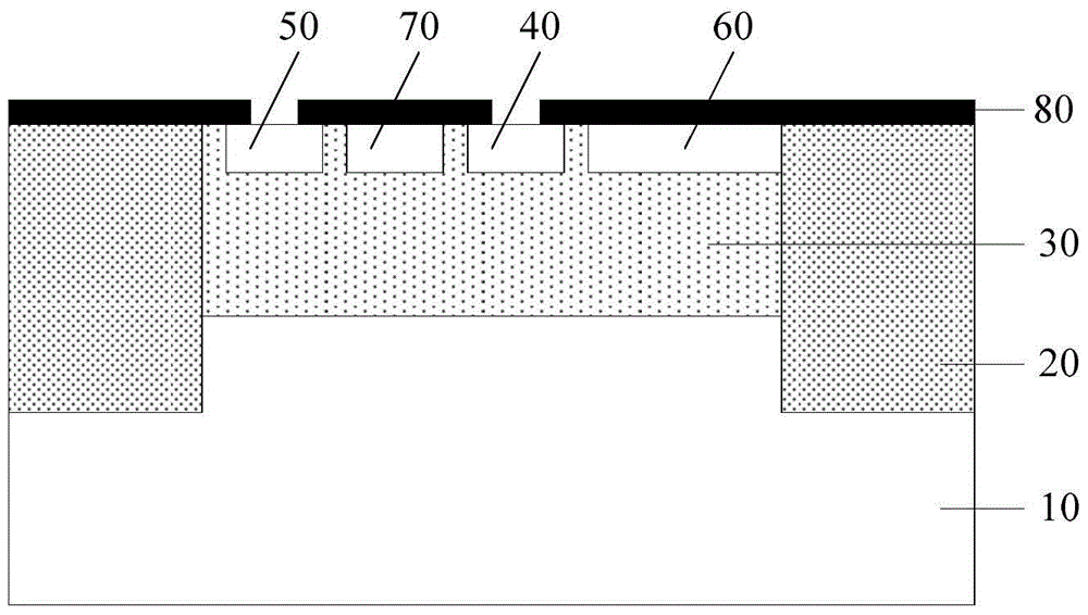
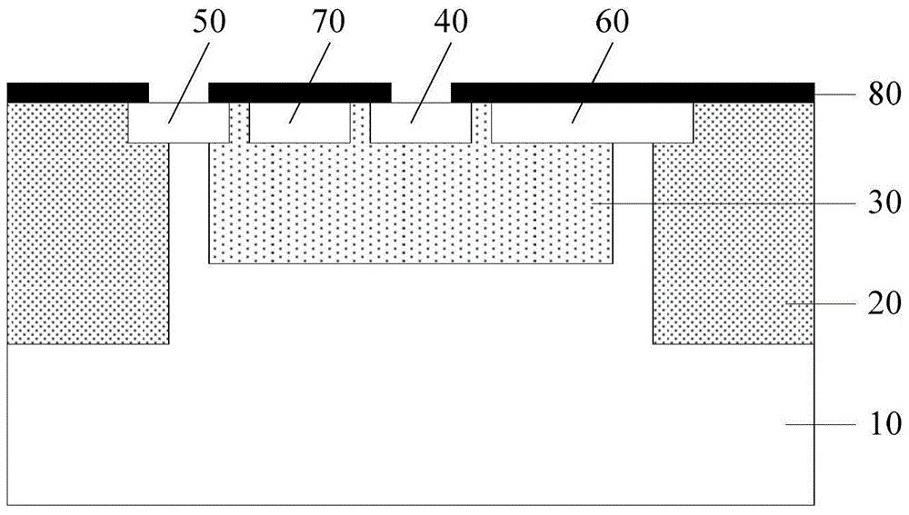
[0035] An embodiment of the present invention provides a CMOS image sensor, including a plurality of pixel units arranged in an array. Such as figure 2 with image 3 As shown, each pixel unit of the CMOS image sensor may include: a P-type semiconductor substrate 10; a first N-type ion layer 30 located above the P-type semiconductor substrate 10, and surrounding the first N-type The P well 20 of the ion layer 30; the second N-type ion layer 40 and the third ...
PUM
 Abstract
Description
Claims
Application Information