Array substrate of TFT-LCD (Thin Film Transistor-Liquid Crystal Display) and manufacturing method thereof

An array substrate and substrate technology, applied in the field of liquid crystal displays, can solve the problems of excessive storage capacitance, slow pixel charging speed, large storage capacitance, etc., and achieve the effects of reducing storage capacitance, reducing overlapping area, and improving chromatic aberration

Active Publication Date: 2014-12-24
BOE TECH GRP CO LTD +1
View PDF3 Cites 0 Cited by
  • Summary
  • Abstract
  • Description
  • Claims
  • Application Information

AI Technical Summary

Problems solved by technology

figure 2 In the array substrate of the planar electric field mode TFT-LCD shown, since two layers of ITO are facing each other, that is, 2ITO and 1ITO overlap and face each other, the storage capacitance is very large, resulting in slow pixel charging speed.
[0004] When realizing the technical solution of the present invention, the inventors found that the array substrate of the TFT-LCD in the planar electric field mode provided by the prior art has too large storage capacitance. The problem is especially obvious

Method used


Image

  • Array substrate of TFT-LCD (Thin Film Transistor-Liquid Crystal Display) and manufacturing method thereof
  • Array substrate of TFT-LCD (Thin Film Transistor-Liquid Crystal Display) and manufacturing method thereof
  • Array substrate of TFT-LCD (Thin Film Transistor-Liquid Crystal Display) and manufacturing method thereof

Examples


Embodiment Construction

[0039] The following will clearly and completely describe the technical solutions in the embodiments of the present invention with reference to the accompanying drawings in the embodiments of the present invention. Obviously, the described embodiments are some of the embodiments of the present invention, but not all of them. Based on the embodiments of the present invention, all other embodiments obtained by persons of ordinary skill in the art without making creative efforts belong to the protection scope of the present invention.

[0040] Embodiments of the present invention provide a TFT-LCD array substrate and a manufacturing method thereof, which can reduce storage capacitance and chromatic aberration, and have better process realization.

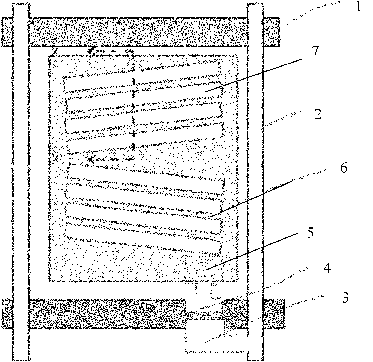
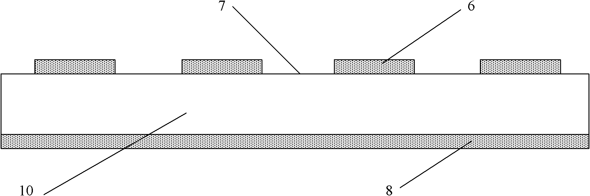
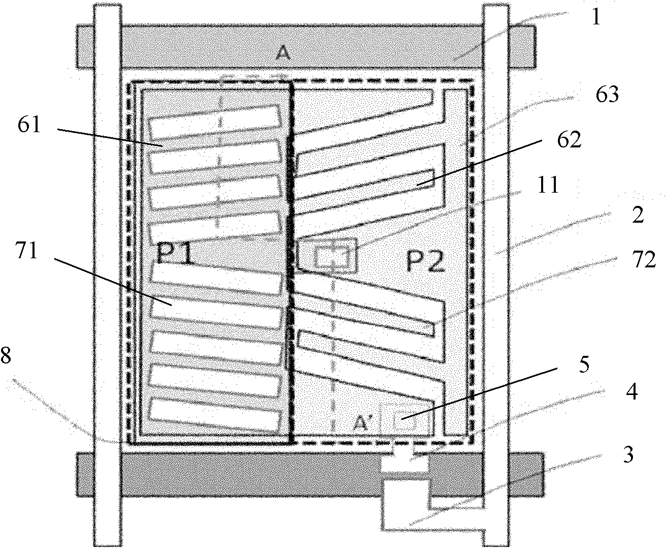
[0041] An embodiment of the present invention provides an array substrate of a TFT-LCD, such as image 3 and Figure 4 As shown, the array substrate includes: a substrate, a gate line and a data line formed on the substrate; the inter...


PUM


Abstract

The present disclosure provides an array substrate for a thin film transistor liquid crystal display (TFT-LCD), comprising: a base substrate having gate lines and data lines intersecting with each other to define sub-pixel units, each comprising a thin film transistor, a common electrode, a first pixel region and a second pixel region, wherein the first pixel region includes a first pixel electrode connected to the common electrode and a second pixel electrode connected to a drain electrode of the thin film transistor, and the first pixel electrode is on a same layer as and insulated from the second pixel electrode, and wherein the second pixel region includes a third pixel electrode connected to the common electrode and a fourth pixel electrode connected to the drain electrode, which are on a same layer and spaced apart from each other by a second local opening.

Description

technical field [0001] The present invention relates to the field of liquid crystal displays, in particular to an array substrate of a Thin Film Transistor-Liquid Crystal Display (TFT-LCD for short) and a manufacturing method thereof. Background technique [0002] Among liquid crystal displays of TN, IPS, VA and planar electric field modes, the planar electric field mode has the advantages of wide viewing angle, low chromatic aberration, and high transmittance, and is increasingly adopted by major panel manufacturers. [0003] However, the process sequence of the planar electric field mode thin film transistor liquid crystal display in the array process section is different from that of other modes of liquid crystal displays. Such as figure 1 and figure 2 As shown, gate line 1 and data line 2 intersect to define a pixel unit. During the manufacturing process, the first layer is the first pixel electrode layer (usually indium tin oxide ITO, which can be called 1ITO) includ...

Claims


Application Information

Patent Timeline
Patent Type & Authority Patents(China)
IPC IPC(8): G02F1/1343G02F1/1362G02F1/1368H01L27/12H01L21/77
CPCG02F2001/134345G02F2001/134372G02F1/134363G02F1/134345G02F1/134372G02F1/136295G02F1/133345G02F1/134309G02F1/13439G02F1/136227G02F1/136286G02F1/1368G02F2201/121G02F2201/123
Inventor 孙荣阁
Owner BOE TECH GRP CO LTD
Why Eureka
Try Eureka