
OLED array substrate and OLED display device

a technology of organic lightemitting diodes and array substrates, applied in the field of display, can solve the problems of difficult to further improve ppi, high density, and disadvantages of a larger ppi circuit design, and achieve the effects of improving image display uniformity, facilitating circuit design, and increasing pixel density

Active Publication Date: 2021-12-07
WUHAN CHINA STAR OPTOELECTRONICS SEMICON DISPLAY TECH CO LTD
View PDF5 Cites 0 Cited by
  • Summary
  • Abstract
  • Description
  • Claims
  • Application Information

AI Technical Summary

Benefits of technology

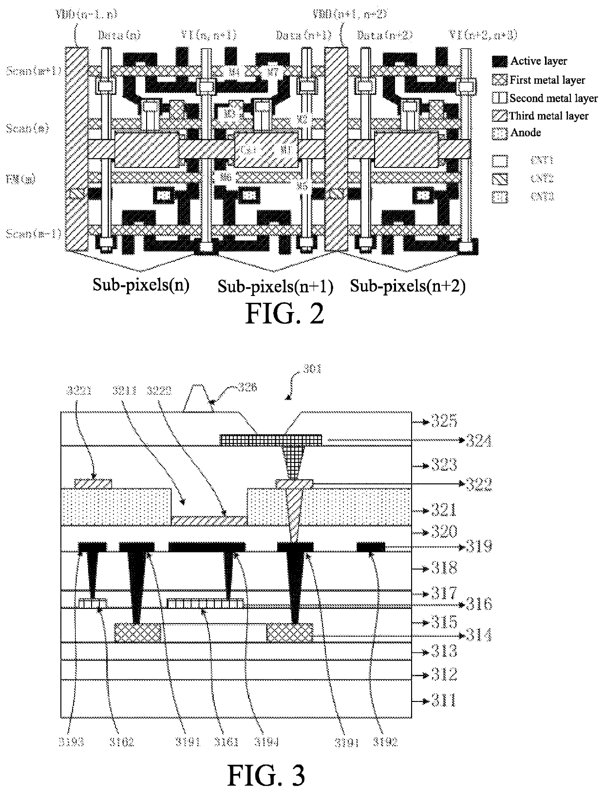
The present patent provides an OLED array substrate and OLED display device that allow for greater pixel density, increased image display uniformity, reduced coupling storage capacitance between lines, and formed a larger storage capacitance. The OLED array substrate includes a plurality of driving circuits of a plurality sub-pixels using a mirror symmetrical structure, and a plurality of reset signal lines and a plurality of power signal lines extending along a same direction. By sharing each of the reset signal lines and each of a plurality of first vias, and sharing each of the power signal lines and each of a plurality of second vias, about half of lines of power signal lines, reset signal lines, and vias are saved. This allows for realizing high PPI panel designs. The design includes a GE1 / SD1 / SD2 three-layer structure design for metal lines, which further facilitates a larger PPI circuit design and increases image display uniformity.

Problems solved by technology

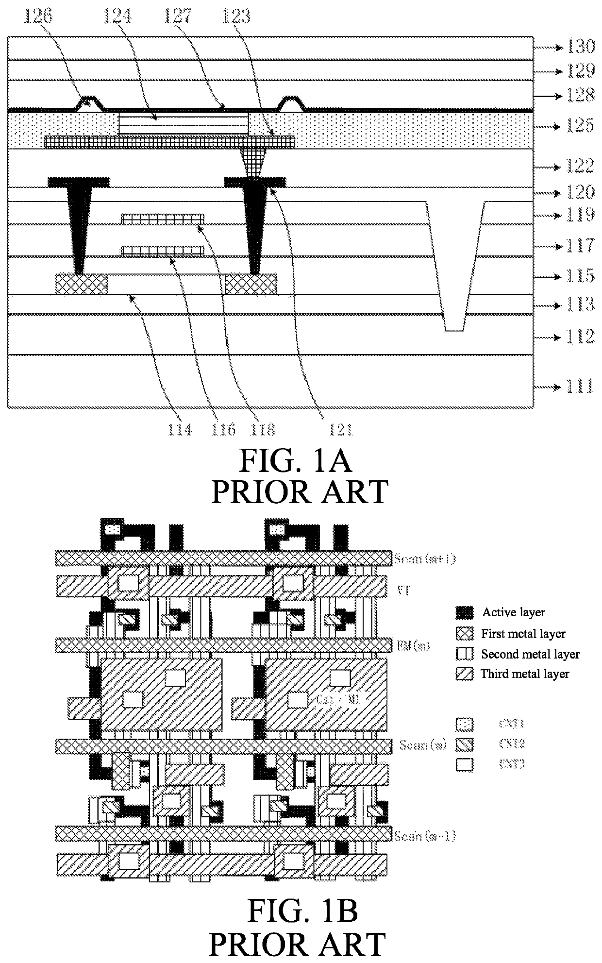
The gate electrode of the driving TFT of the first gate electrode layer also serves as the lower plate of the storage capacitor, which is disadvantageous for a larger PPI circuit design.
A number of lines and a number of vias CNT are large, a density is high, and PPI is difficult to be further improved.

Method used


Image

  • OLED array substrate and OLED display device
  • OLED array substrate and OLED display device

Examples


Embodiment Construction

[0018]Embodiments of the present disclosure are described in detail below and examples of the embodiments are illustrated in the accompanying drawings, wherein same or similar labels throughout the present disclosure represent corresponding same or similar elements or corresponding elements having same or similar functions. The description of the embodiments with reference to the accompanying drawings below is exemplary, aims at illustrating the present disclosure, and cannot be considered as limitations to the present disclosure.

[0019]In the present disclosure, unless otherwise definitely specified and defined, when a first feature is “over” or “under” a second feature, the first feature may be directly in contact with the second feature, or the first feature and the second feature may not be directly in contact with each other and may be in contact through another feature between the first feature and the second feature. Furthermore, when the first feature is “over”, “above”, or “...


PUM

PropertyMeasurementUnit
luminanceaaaaaaaaaa
poweraaaaaaaaaa
electric fieldsaaaaaaaaaa

Abstract

An organic light-emitting diode (OLED) array substrate and an OLED display device are provided. The OLED array substrate includes a plurality of driving circuits of a plurality of sub-pixels using a mirror symmetrical structure, and a plurality of reset signal lines and a plurality of power signal lines extending along a same direction. By sharing each of the reset signal lines and each of a plurality of first vias, and sharing each of the power signal lines and each of a plurality of second vias, about half of lines of power signal lines, reset signal lines, and vias are saved. Therefore, room for increasing pixels per inch (PPI) is provided, facilitating realizing high PPI panel designs.

Description

FIELD OF INVENTION[0001]The present disclosure relates to a technical field of displays, and more particularly to an organic light-emitting diode (OLED) array substrate and an OLED display device.BACKGROUND OF INVENTION[0002]Recently, rapid development of organic light emitting diode (OLED) display technologies has promoted fast entry of curved surface and flexible touch display products into the market. Relevant technologies also update with each passing day. OLEDs are diodes that use organic semiconductor material and light emitting material driven by electric fields to cause light emission through carrier injection and recombination. OLED display devices have advantages of being lightweight and self-luminous, and having large viewing angles, low driving voltage, high luminous efficiency, low power consumption, fast response speed, etc., thereby having a wider and wider application scope.[0003]Active-matrix organic light emitting diode (AMOLED) display devices are display devices ...

Claims


Application Information

Patent Timeline
Patent Type & Authority Patents(United States)
IPC IPC(8): H01L29/08H01L27/32H01L27/12
CPCH01L27/3276H01L27/3262H01L27/3265H01L27/1214H10K59/131H10K59/1213H10K59/1216
Inventor WANG, WEIHUANG, QING
Owner WUHAN CHINA STAR OPTOELECTRONICS SEMICON DISPLAY TECH CO LTD
Learn More