Optoelectronic Semiconductor Device, Method for Producing an Optoelectronic Semiconductor Device, and Light Source Comprising an Optoelectronic Semiconductor Device

a technology of optoelectronic semiconductors and semiconductor devices, which is applied in the direction of semiconductor devices, basic electric elements, electrical apparatus, etc., can solve the problems of sensitive converter materials that may react sensitively to temperature fluctuations and be impaired, and achieve good color rendering, good filling, and large color gamut

Active Publication Date: 2017-05-11
OSRAM OLED
View PDF10 Cites 7 Cited by
  • Summary
  • Abstract
  • Description
  • Claims
  • Application Information

AI Technical Summary

Benefits of technology

[0018]According to at least one embodiment of the optoelectronic semiconductor device, the conversion element comprises wavelength-converting quantum dots as sensitive wavelength-converting converter material. The conversion element is formed, for example, with a matrix material, wherein the wavelength-converting quantum dots have been introduced into the matrix material. The conversion element may thus be a potting body containing the quantum dots. The potting body is preferably formed of a material which, for example, by means of casting, is processed into the final product in liquid form and solidified as said final product. Production by casting may lead to good filling and / or sealing of any cavities present and / or to form-fitting overmolding of cast materials. For example, the matrix material may be formed with silicone, acrylate, epoxy resin, polycarbonate or a sol-gel material.
[0019]Through the use of quantum dots as the converter material, good color rendering may be achieved, since the converted electromagnetic radiation is relatively narrowband and thus no mixing of different spectral colors arises. For example, the spectrum of the converted radiation has a wavelength width of at least 20 nm to at most 35 nm. This allows the generation of light whose color may be assigned very precisely to a region of the spectrum. In this way, when the optoelectronic semiconductor device is used in a display, a large color gamut may be achieved, since, for example, a narrow-band green- and a narrow-band red-converting converter may be used instead of a broadband yellow-converting converter, so enabling greater color coverage.

Problems solved by technology

Furthermore, the sensitive converter material may react sensitively to temperature fluctuations and be impaired, for example, in its functionality by such temperature fluctuations.

Method used


Image

  • Optoelectronic Semiconductor Device, Method for Producing an Optoelectronic Semiconductor Device, and Light Source Comprising an Optoelectronic Semiconductor Device
  • Optoelectronic Semiconductor Device, Method for Producing an Optoelectronic Semiconductor Device, and Light Source Comprising an Optoelectronic Semiconductor Device
  • Optoelectronic Semiconductor Device, Method for Producing an Optoelectronic Semiconductor Device, and Light Source Comprising an Optoelectronic Semiconductor Device

Examples


Embodiment Construction

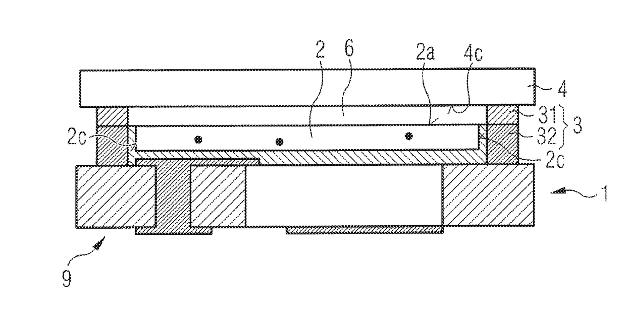
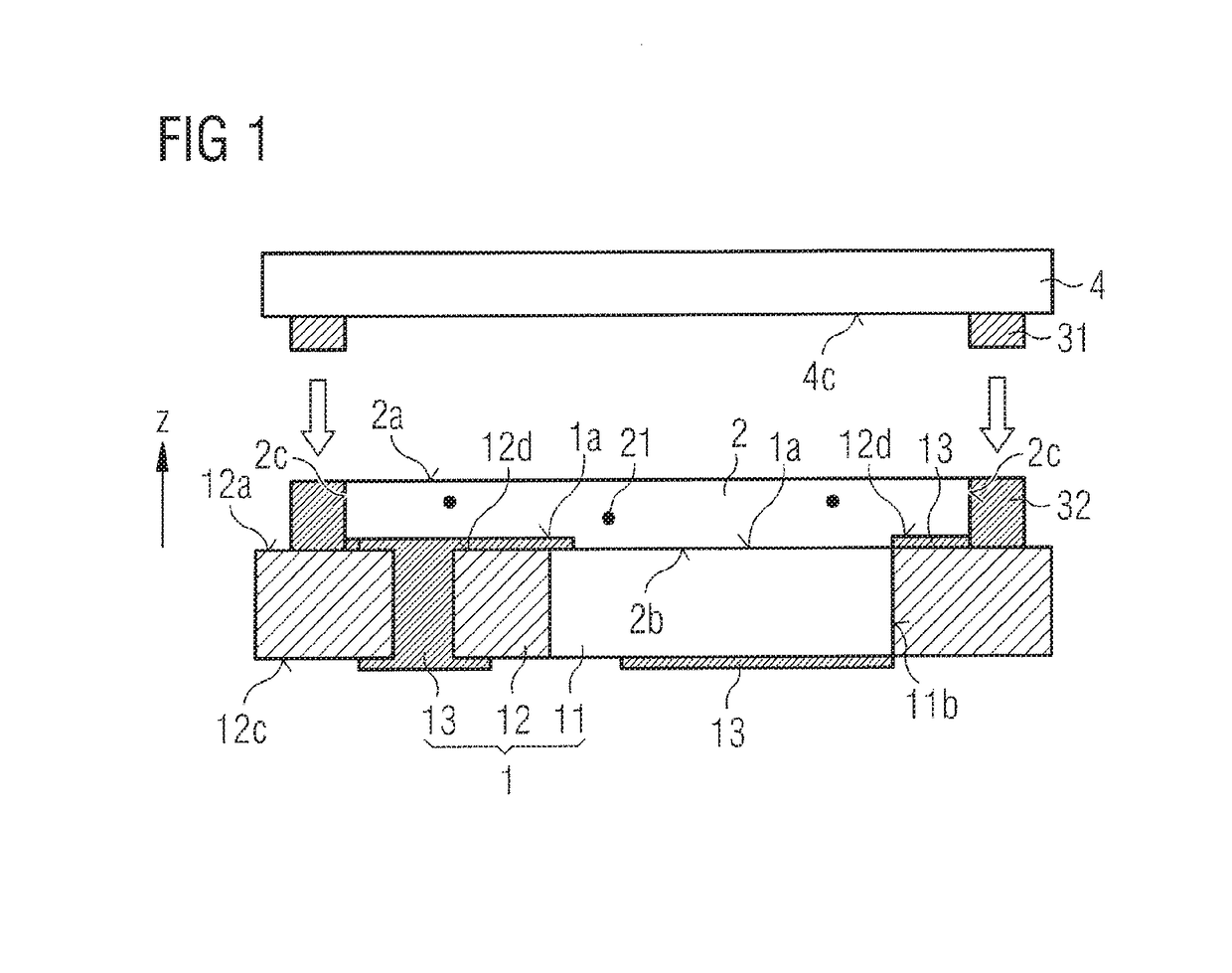
[0079]On the basis of the schematic sectional representation of FIG. 1, a method step of a method described here for producing an optoelectronic semiconductor device 9 is explained in greater detail. In the method, first of all a light-emitting diode component 1 having at least one light-emitting diode chip 11 and a top face 1a is provided. The top face 1a is arranged downstream of the light-emitting diode component 1 in an emission direction Z.

[0080]The light-emitting diode component 1 further comprises a molding 12 and connection points 13. The molding 12 here encloses the light-emitting diode chip 11 at the lateral side faces 11b thereof. The connection points 13 pass right through the molding 12 and extend at least in part on a bottom face 12C and / or a top face 12a of the molding 12. It is however—other than is shown in the figures—also possible for the connection points to be mounted on a laterally located side face of the molding 12 and for the molding 12 to completely cover a...


PUM


Abstract

An optoelectronic semiconductor device, a method for manufacturing an optoelectronic semiconductor device and light source having an optoelectronic semiconductor device are disclosed. In an embodiment, an optoelectronic semiconductor device includes a light-emitting diode component having at least one light-emitting diode chip and a top face, the top face arranged downstream of the light-emitting diode chip in an emission direction, wherein the light-emitting diode component further includes a molding and connection points, a conversion element arranged downstream of the light-emitting diode component in the emission direction, the conversion element includes wavelength-converting quantum dots, a frame member enclosing all side faces of the conversion element in a frame-like manner and a cover member arranged downstream of the conversion element in the emission direction, the cover member including a radiation-transmissive material, wherein the cover member covers the conversion element at a top face remote from the light-emitting diode chip.

Description

[0001]This patent application is a national phase filing under section 371 of PCT / EP2015 / 063093, filed Jun. 11, 2015, which claims the priority of German patent application 10 2014 108 282.6, filed Jun. 12, 2014, each of which is incorporated herein by reference in its entirety.BACKGROUND[0002]Document DE 10 2012 110 668 describes an optoelectronic semiconductor device and a method for producing such an optoelectronic semiconductor device.[0003]One problem addressed consists in providing an optoelectronic semiconductor device with a sensitive converter material and a light source with such an optoelectronic semiconductor device, each of which have an elevated service life. A further problem addressed consists in providing a method for producing an optoelectronic semiconductor device with a sensitive converter material.SUMMARY OF THE INVENTION[0004]Embodiments of the invention provide an optoelectronic semiconductor device. The optoelectronic semiconductor device, for example, compri...

Claims


Application Information

Patent Timeline
Patent Type & Authority Applications(United States)
IPC IPC(8): H01L33/54H01L33/48H01L33/50
CPCH01L33/54H01L33/507H01L33/486H01L33/502H01L33/44H01L33/483H01L33/58
Inventor VON MALM, NORWIN
Owner OSRAM OLED
Why Eureka
Try Eureka